What is a CCD matrix?
CCD / Charge-Coupled Device or CCD / Device with charge bond- it's analog integrated circuit, which includes light-sensitive photodiodes made of silicon or tin oxide. The principle of operation of this microcircuit is based on the technology of charge-coupled devices (CCDs).
History of the CCD
For the first time, a charge-coupled device was used by George Smith and Willard Boyle at Bell Laboratories of the US largest corporation AT & T Bell Labs in 1969. They conducted research in the field of video telephony and the so-called "semiconductor bubble memory".
Soon, miniature devices became quite widespread and began to be used as memory devices in which the charge was placed in the input register of the microcircuit. After some time, the ability of the memory element to receive a charge due to the photoelectric effect became the main purpose of the use of CCD devices.
A year later, in 1970, the researchers of the same Laboratory were able to capture images using the simplest linear devices, which was actually adopted by Sony engineers. This company is still actively working in the field of CCD technologies, investing huge financial investments in this area, in every possible way developing the production of CCD matrices for its video cameras. By the way, the CCD chip was installed on the tombstone of Sony CEO Kazuo Iwama, who died in 1982. After all, it was he who stood at the origins of the start of mass production of a CCD matrix.
The contribution of the inventors of the CCD matrix did not go unnoticed, so in 2006 Willard Boyle and George Smith received an award from the US National Academy of Engineering for their developments in this area, and in 2009 they were awarded the Nobel Prize in Physics.
The principle of operation of the CCD matrix
The CCD-matrix is almost completely made of polysilicon, which was initially separated from the silicon substrate by a special membrane. When voltage is applied to the membrane by means of polysilicon gates, the electrical potentials located near the conductor electrodes change greatly.
Before exposure and applying a certain voltage power to the electrodes, all the charges that were formed earlier are reset, and all elements are transformed into an identical or original state.
The combination of voltages on the electrodes creates a potential reserve or a so-called well, where electrons accumulate, which appeared in a certain pixel of the matrix during exposure under the influence of light rays. Depending on the intensity of the force luminous flux the volume of accumulated electrons in the potential well is also located, so the larger it is, the higher the power of the final charge of a certain pixel will be.
After the exposure is completed, successive changes in the supply voltage of the electrodes occur in each individual pixel, next to which a potential distribution is observed, as a result of which the charges move in a given direction - to the output pixels of the CCD matrix.
Composition of CCD-matrix elements
In general terms, the design of a CCD element can be represented as a p-type silicon substrate equipped with channels from an n-type semiconductor. Above these channels are polycrystalline silicon electrodes with an insulating silicon oxide membrane.
After applying the electric potential to these electrodes, a potential trap (well) appears in the weakened zone under the n-type channel. Its main task is to conserve electrons. A particle of light entering silicon provokes the generation of electrons, which are attracted by the potential trap and remain in it. A large number of photons or bright light provides a powerful charge to the trap, after which it is necessary to calculate and amplify the value of the resulting charge, which experts call photocurrent.
The process of reading the photocurrents of CCD-elements is carried out with the so-called sequential shift registers, which convert a row of charges at the input into a train of pulses at the output. This thread pulses is actually an analog signal that is fed to the amplifier.
Thus, in analog signal it is possible to convert string charges from CCD elements using a register. In practice, the sequential shift register in CCD-matrices is performed by means of all the same CCD-elements built in one line. At the same time, work this device is based on the ability of charge-coupled devices to exchange the charges of their potential traps. This process is carried out due to the presence of specialized transfer electrodes, which are placed between adjacent CCD elements. At the moment of applying an increased potential to the nearest electrode, the charge passes under it from the potential well. At the same time, two or four transfer electrodes are usually located between the CCD elements, the number of which determines the phase of the shift register, called two-phase, three-phase or four-phase.
The supply of different potentials to the transfer electrodes is synchronized in such a way that the transition of the charges of potential traps of all CCD elements of the register is performed almost simultaneously. So in one "step" of transfer, CCD elements move charges along the chain from right to left or from left to right. In this case, the extreme CCD element gives its charge to the amplifier, which is located at the output of the register. Thus, it becomes quite obvious that a serial shift register is a serial output, parallel input device.
After the process of reading absolutely all charges from the register is completed, it becomes possible to apply to its input new line, then another, and so on. The result is a continuous analog signal based on a two-dimensional photocurrent flow. Thereafter, the parallel input stream to the serial shift register is provided by a collection of vertically oriented serial shift registers, referred to as the parallel shift register. This entire structure, when assembled, is precisely the device called today a CCD-matrix.
For the first time, the principle of a CCD with the idea of storing and then reading electronic charges was developed by two BELL engineers in the late 60s in the course of searching for new types of memory for computers that could replace the memory on ferrite rings (yes, there was such a memory). This idea turned out to be unpromising, but the ability of silicon to respond to the visible spectrum of radiation was noticed and the idea to use this principle for image processing was developed.
Let's start with the definition of the term.
The abbreviation CCD means "Charge-Coupled Devices" - this term was formed from the English "Charge-Coupled Devices" (CCD).
This type of device currently has a very wide range of applications in a variety of optoelectronic devices for image recording. In everyday life, these are digital cameras, camcorders, various scanners.
What distinguishes a CCD receiver from a conventional semiconductor photodiode, which has a photosensitive area and two electrical contacts for picking up an electrical signal?
Firstly, such photosensitive areas (often called pixels - elements that receive light and convert it into electric charges) in a CCD receiver is very large, from several thousand to several hundred thousand and even several million. The sizes of individual pixels are the same and can be from units to tens of microns. Pixels can be lined up in one row - then the receiver is called a CCD-line, or fill a surface area in even rows - then the receiver is called a CCD-matrix.
Arrangement of light-receiving elements (rectangles of blue color) in a CCD ruler and a CCD matrix.
Secondly, in a CCD receiver, which looks like a conventional microcircuit, there is no huge number of electrical contacts for outputting electrical signals, which, it would seem, should come from each light-receiving element. But it connects to the CCD receiver electronic circuit, which allows you to extract from each photosensitive element an electrical signal proportional to its illumination.
The action of a CCD can be described as follows: each light-sensitive element - a pixel - works like a piggy bank for electrons. Electrons are generated in pixels by the action of light coming from a source. Over a given period of time, each pixel gradually fills with electrons in proportion to the amount of light that enters it, like a bucket outside when it rains. At the end of this time, the electric charges accumulated by each pixel are transferred in turn to the "output" of the device and measured. All this is possible due to a certain structure of the crystal, where light-sensitive elements are placed, and electrical circuit management.
The CCD matrix works almost exactly the same way. After exposure (illumination by the projected image), the electronic control circuit of the device supplies a complex set of impulse voltage, which begin to shift the columns with electrons accumulated in pixels to the edge of the matrix, where a similar measuring CCD register is located, the charges in which are already shifted in the perpendicular direction and fall on the measuring element, creating signals in it proportional to individual charges. Thus, for each subsequent moment of time, we can get the value of the accumulated charge and figure out which pixel on the matrix (row number and column number) it corresponds to.
Briefly about the physics of the process.
To begin with, we note that CCDs are products of the so-called functional electronics. They cannot be represented as a collection of individual radio elements - transistors, resistances and capacitors. The work is based on the principle of charge bonding. The principle of charge coupling uses two positions known from electrostatics:
- like charges repel each other
- Charges tend to settle down where their potential energy is minimal. Those. rudely - "the fish is looking for where it is deeper."
Let's start with a MOS capacitor (MOS is short for metal-oxide-semiconductor). This is what remains of the MOSFET if you remove the drain and source from it, that is, just an electrode separated from silicon by a layer of dielectric. For definiteness, we assume that the semiconductor is p-type, i.e., the concentration of holes under equilibrium conditions is much (several orders of magnitude) greater than that of electrons. In electrophysics, a “hole” is a charge that is inverse to the charge of an electron, i.e. positive charge.
What will happen if a positive potential is applied to such an electrode (it is called a gate)? The electric field created by the gate, penetrating the silicon through the dielectric, repels the moving holes; a depleted region appears - a certain volume of silicon, free from the majority carriers. With the parameters of semiconductor substrates typical for CCDs, the depth of this region is about 5 μm. On the contrary, the electrons that have arisen here under the action of light will be attracted to the gate and will accumulate at the oxide-silicon interface directly under the gate, i.e., fall into a potential well (Fig. 1).

Rice. 1
Formation of a potential well when voltage is applied to the gate
In this case, as electrons accumulate in the well, they partially neutralize the electric field created in the semiconductor by the gate, and in the end they can completely compensate for it, so that the entire electric field will fall only on the dielectric, and everything will return to the initial state- except that a thin layer of electrons is formed at the interface.
Let now another gate be located next to the gate, and a positive potential is also applied to it, moreover, a larger one than to the first one (Fig. 2). If only the gates are close enough, their potential wells are combined, and the electrons in one potential well move to the adjacent one if it is "deeper". 
Rice. 2
Overlapping potential wells of two closely spaced gates. The charge flows to the place where the potential well is deeper.
Now it should be clear that if we have a chain of gates, then it is possible, by applying appropriate control voltages to them, to transfer a localized charge packet along such a structure. A remarkable property of CCDs, the self-scanning property, is that only three clock buses are sufficient to drive a chain of gates of any length. (The term bus in electronics is a conductor electric current, connecting elements of the same type, a clock bus - conductors through which a phase-shifted voltage is transmitted.) Indeed, for the transfer of charge packets, three electrodes are necessary and sufficient: one transmitting, one receiving and one insulating, separating pairs of receiving and transmitting from each other, and of the same name the electrodes of such triplets can be connected to each other into a single clock bus, requiring only one external output (Fig. 3).

Rice. 3
The simplest three-phase CCD register.
The charge in each potential well is different.
This is the simplest three-phase CCD shift register. Clock diagrams of the operation of such a register are shown in Fig. 4.


Rice. 4
Clock diagrams for controlling a three-phase register are three meanders shifted by 120 degrees.
When the potentials change, charges move.
It is clear that for him normal operation at any given time, at least one clock bus must be high and at least one must be low (barrier potential). When the potential rises on one bus and decreases on the other (previous) one, all charge packets are simultaneously transferred to neighboring gates, and beyond full cycle(one cycle on each phase bus), the charge packets are transferred (shifted) to one element of the register.
To localize the charge packets in the transverse direction, so-called stop channels are formed - narrow strips with an increased concentration of the main dopant, which run along the transfer channel (Fig. 5).

Rice. 5.
View of the register from above.
The transfer channel in the lateral direction is limited by the stop channels.
The fact is that the concentration of the dopant determines at what specific voltage on the gate a depletion region forms under it (this parameter is nothing more than the threshold voltage of the MOS structure). From intuitive considerations, it is clear that the greater the impurity concentration, i.e., the more holes in the semiconductor, the more difficult it is to drive them deep, i.e., the higher the threshold voltage or, at one voltage, the lower the potential in the potential well.
Problems
If in the production of digital devices the spread of parameters across the plate can reach several times without a noticeable effect on the parameters of the resulting devices (since the work is done with discrete voltage levels), then in a CCD, a change in, say, the dopant concentration by 10% is already noticeable in the image. The size of the crystal adds its own problems, as well as the impossibility of redundancy, as in memory LSI, so that defective areas lead to the unusability of the entire crystal.
Outcome
Different pixels of a CCD matrix technologically have different sensitivity to light, and this difference must be corrected.
In digital CMAs, this correction is called the Auto Gain Control (AGC) system.
How the AGC system works
For simplicity, we will not take anything specific. Let's assume that there are some potential levels at the output of the ADC of the CCD node. Let's say 60 is the average white level.
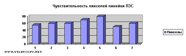

- For each pixel of the CCD line, the value is read when it is illuminated with reference white light (and in more serious devices, the “black level” is also read).
- The value is compared to a reference level (eg average).
- The difference between the output value and the reference level is stored for each pixel.
- In the future, when scanning, this difference is compensated for each pixel.
The AGC system is initialized each time the scanner system is initialized. You probably noticed that when you turn on the machine, after some time, the scanner carriage starts to make forward-return movements (crawl at the b/w strip). This is the initialization process of the AGC system. The system also takes into account the condition of the lamp (aging).
You also probably noticed that small MFPs equipped with a color scanner “light the lamp” in three colors in turn: red, blue and green. Then only the backlight of the original turns white. This is done to better correct the sensitivity of the matrix separately for the RGB channels.
Halftone Test (SHADING TEST) allows you to initiate this procedure at the request of the engineer and bring the correction values to real conditions.
Let's try to consider all this on a real, "combat" machine. We take as a basis a well-known and popular device SAMSUNG SCX-4521 (Xerox Pe 220).
It should be noted that in our case, CCD becomes CIS (Contact Image Sensor), but the essence of what is happening fundamentally does not change from this. Just as a light source, a line of LEDs is used.
So:
The image signal from the CIS has a level of about 1.2 V and is fed to the ADC section (ADCP) of the device controller (ADCP). After the SADC, the analog CIS signal will be converted to an 8-bit digital signal.
The image processor in the SADC first uses the tone correction function and then the gamma correction function. After that, the data is fed to different modules according to the mode of operation. Text mode sends image data to the LAT module, Photo mode sends image data to the "Error Diffusion" module, PC-Scan mode sends image data directly to Personal Computer through DMA access.
Before testing, place a few clean sheets white paper. It goes without saying that the optics, the b/w stripe, and the scanner assembly in general, must be “licked” from the inside first.
- Select in TECH MODE
- Press the ENTER button to scan the image.
- After scanning, "CIS SHADING PROFILE" (CIS halftone profile) will be printed. An example of such a sheet is shown below. It doesn't have to be a copy of your result, but close in image.
- If the printed image is very different from the image shown in the figure, then the CIS is faulty. Please note that “Results: OK” is written at the bottom of the report sheet. This means that the system has no serious claims to the CIS module. Otherwise, error results will be given.
Profile printout example:

Good luck to you!!
Materials of articles and lectures of teachers from St. Petersburg State University (LSU), St. Petersburg Electrotechnical University (LETI) and Axl are taken as a basis. Thank them.
Material prepared by V. Shelenberg
Matrix is the main structural element camera and one of the key parameters taken into account by the user when choosing a camera. Matrices of modern digital cameras can be classified according to several prosigns, but the main and most common is the division of matrices according to charge reading method, on: matrices CCD type and CMOS matrices. In this article, we will consider the principles of operation, as well as the advantages and disadvantages of these two types of matrices, since they are widely used in modern photo and video equipment.
CCD matrix
Matrix CCD also called CCD(Charge-Coupled Devices). CCD the matrix is a rectangular plate of light-sensitive elements (photodiodes) located on a silicon semiconductor crystal. The principle of its operation is based on the line-by-line movement of charges that have accumulated in the gaps formed by photons in silicon atoms. That is, upon collision with a photodiode, a photon of light is absorbed and an electron is released (an internal photoelectric effect occurs). As a result, a charge is formed, which must somehow be stored for further processing. For this purpose, a semiconductor is embedded in the silicon substrate of the matrix, above which a transparent electrode made of polycrystalline silicon is located. And as a result of applying an electric potential to this electrode in the depleted zone under the semiconductor, a so-called potential well is formed, in which the charge received from photons is stored. When reading an electric charge from the matrix, the charges (stored in potential wells) are transferred along the transfer electrodes to the edge of the matrix (serial shift register) and towards the amplifier, which amplifies the signal and transmits it to the analog-to-digital converter (ADC), from where the converted signal is sent to a processor that processes the signal and saves the resulting image to a memory card .
Polysilicon photodiodes are used to manufacture CCD matrices. Such matrices are small in size and allow you to get enough high quality photos when shooting under normal lighting.
Benefits of CCDs:
- The design of the matrix provides a high density of photocells (pixels) on the substrate;
- High efficiency (the ratio of registered photons to their total number is about 95%);
- High sensitivity;
- Good color rendering(with sufficient lighting).
Disadvantages of CCD matrices:
- High noise at high ISO (at low ISO, the noise level is moderate);
- Low speed work in comparison with CMOS matrices;
- High power consumption;
- More complex signal reading technology, since many control microcircuits are needed;
- Production is more expensive than CMOS matrices.
Matrix CMOS, or CMOS sensor(Complementary Metal Oxide Semiconductors) uses active point sensors. Unlike CCDs, CMOS sensors contain a separate transistor in each photosensitive element (pixel), resulting in charge conversion being performed directly in the pixel. The resulting charge can be read from each pixel individually, so there is no need for charge transfer (as is the case with CCDs). The CMOS pixels are integrated directly with an analog-to-digital converter or even with a processor. This smart technology results in energy savings due to shorter chains of operations compared to CCD matrices, as well as lower cost of the device due to a simpler design.

Brief principle operation of the CMOS sensor: 1) Before shooting, a reset signal is applied to the reset transistor. 2) During exposure, light penetrates through the lens and filter to the photodiode, and as a result of photosynthesis, a charge accumulates in the potential well. 3) The value of the received voltage is read. 4) Data processing and image saving.
Advantages of CMOS sensors:
- Low power consumption (especially in standby modes);
- High performance;
- Requires less production costs, due to the similarity of technology with the production of microcircuits;
- The unity of technology with other digital elements, which allows you to combine analog, digital and processing parts on one crystal (that is, in addition to capturing light in a pixel, you can convert, process and clean the signal from noise).
- The ability to randomly access each pixel or group of pixels, which can reduce the size of the captured image and increase the readout speed.
Disadvantages of CMOS matrices:
- The photodiode occupies a small area of the pixel, resulting in a low light sensitivity of the matrix, but in modern CMOS matrices this minus is practically eliminated;
- The presence of thermal noise from heating transistors inside the pixel during the reading process.
- Relatively large dimensions, fluoroequipment with this type of matrices is characterized by large weight and dimensions.
In addition to the above types, there are also three-layer matrices, each layer of which is a CCD. The difference is that the cells can simultaneously perceive three colors, which are formed by dichroic prisms when a beam of light hits them. Then each beam is directed to a separate matrix. As a result, the brightness of blue, red and green colors is determined on the photocell at once. Three-layer matrices are used in video cameras high level, which have a special designation - 3CCD.
Summing up, I would like to note that with the development of technologies for the production of CCD and CMOS matrices, their characteristics also change, so it is more and more difficult to say which of the matrices is definitely better, but at the same time, CMOS matrices have become increasingly popular in the production of SLR cameras. Based on the characteristic features of various types of matrices, one can get a clear idea why professional photographic equipment that provides high-quality shooting is rather bulky and heavy. This information should be remembered when choosing a camera - that is, take into account the physical dimensions of the matrix, and not the number of pixels.
Solid-state photoelectric converters (SFECs) of images are analogues of transmitting CRTs.
TFECs date back to 1970, with the so-called CCDs and are formed on the basis of individual cells, which are MIS or MOS capacitors. One of the plates of such an elementary capacitor is a metal film M, the second is a semiconductor substrate P ( p- or n-conductivity), the dielectric D is a semiconductor deposited in the form of a thin layer on the substrate P. Silicon doped with an acceptor ( p-type) or donor ( n-type) impurity, and as D - silicon oxide SiO 2 (see fig.8.8).
Rice. 8.8. MOS Capacitor

Rice. 8.9. Movement of charges under the influence of an electric field

Rice. 8.10. Working Principle of Three-Phase CCD System

Rice. 8.11. Movement of charges in a two-phase CCD system
When a voltage is applied to a metal electrode, a “pocket” or a potential well is formed under it, in which minor carriers (in our case, electrons) can “accumulate”, and the majority carriers, holes, will be repelled from M. At some distance from the surface , the concentration of minor carriers may be higher than the concentration of major ones. Near the dielectric D in the substrate P, an inversion layer arises, in which the type of conductivity changes to the reverse one.
The charge package in the CCD can be introduced electrically or with the help of light generation. During light generation, photoelectric processes occurring in silicon will lead to the accumulation of minority carriers in potential wells. The accumulated charge is proportional to the illumination and the accumulation time. Directional charge transfer in a CCD is provided by placing the MOS capacitors so close together that their depletion regions overlap and the potential wells are connected. In this case, the mobile charge of minority carriers will accumulate in the place where the potential well is deeper.
Let under the influence of light the charge accumulated under the electrode U 1 (see Fig.8.9). If now on the adjacent electrode U 2 apply voltage U 2 > U 1 , then another potential well will appear nearby, deeper ( U 2 > U 1). An electric field region will appear between them and minority carriers (electrons) will drift (flow) into a deeper “pocket” (see Fig. 8.9). To eliminate bidirectionality in the transfer of charges, a sequence of electrodes is used, combined in groups of 3 electrodes (see Fig. 8.10).
If, for example, a charge is accumulated under electrode 4 and it is necessary to transfer it to the right, then a higher voltage is applied to the right electrode 5 ( U 2 > U 1) and the charge flows to it, etc.
Almost the entire set of electrodes is connected to three tires:
I - 1, 4, 7, ...
II - 2, 5, 8, ...
III - 3, 6, 9, ...
In our case, the "reception" voltage ( U 2) will be on electrodes 2 and 5, but electrode 2 is separated from electrode 4, where the charge is stored, by electrode 3 (which has
U 3 = 0), so there will be no overflow to the left.
The three-cycle operation of a CCD implies the presence of three electrodes (cells) per TV-image element, which reduces the usable area used by the light flux. To reduce the number of cells (electrodes) of the CCD, metal electrodes and a dielectric layer are formed in a stepped shape (see Fig. 8.11). This allows, when applying voltage pulses to the electrodes, to create potential wells of different depths under its different sections. Most of the charges from the adjacent cell drain into the deeper pit.
With a two-phase CCD system, the number of electrodes (cells) in the matrix is reduced by one third, which favorably affects the reading of the potential relief.
CCDs were originally proposed to be used in computer science as storage devices, shift registers. At the beginning of the chain, an injection diode was placed, introducing a charge into the system, and at the end of the circuit, an output diode, usually this n-p- or p-n- MOS structure transitions, which form field-effect transistors with the first and last electrodes (cells) of CCD chains.
But it soon became clear that CCDs are very sensitive to light, and therefore it is better and more efficient to use them as light detectors, and not as storage devices.
If a CCD array is used as a photodetector, then charge accumulation under one electrode or another can be carried out by an optical method (light injection). It can be said that CCD matrices are inherently light-sensitive analog shift registers. Today, CCDs are not used as storage devices (memory devices), but only as photodetectors. They are used in fax machines, scanners (CCD arrays), cameras and camcorders (CCD arrays). Typically, TV cameras use so-called CCD chips.
We assumed that all 100% of the charges are transferred to the adjacent pocket. However, in practice one has to reckon with losses. One of the sources of losses is "traps" that can capture and hold charges for some time. These charges do not have time to flow into the adjacent pocket if the transfer rate is high.
The second reason is the flow mechanism itself. At the first moment, the charge transfer occurs in a strong electric field - the drift in E. However, as the charges flow, the field strength decreases and the drift process dies out, so the last portion moves due to diffusion, 100 times slower than the drift. Waiting for the last portion means slowing down the performance. Drift gives more than 90% transfer. But it is the last percentages that are the main ones in determining losses.
Let the transfer coefficient of one transfer cycle be equal to k= 0.99, assuming the number of cycles to be N= 100, we determine the total transfer coefficient:
0,99 100 = 0,366
It becomes obvious that when large numbers elements, even insignificant losses on one element become of great importance for the chain as a whole.
Therefore, the question of reducing the number of charge transfers in CCD is especially important. In this respect, the charge transfer coefficient of a two-phase CCD array will be somewhat higher than that of a three-phase system.
What is a CCD?
A bit of history
Photographic materials were previously used as a light receiver: photographic plates, photographic film, photographic paper. Later, television cameras and PMTs (photoelectric multiplier) appeared.
In the late 60s and early 70s, so-called "Charge-Coupled Devices" began to be developed, which is abbreviated as CCD. On English language it looks like "charge-coupled devices" or CCD for short. The principle behind CCDs was the fact that silicon is capable of responding to visible light. And this fact led to the idea that this principle can be used to obtain images of luminous objects.Astronomers were among the first to recognize the extraordinary capabilities of CCDs for imaging. In 1972, a group of researchers from JPL (Jet Propulsion Laboratory, USA) founded the CCD development program for astronomy and space research. Three years later, together with scientists from the University of Arizona, this team obtained the first astronomical CCD image. In a near-infrared image of Uranus, using a 1.5-meter telescope, dark spots were found near the south pole of the planet, indicating the presence of methane there ...
The use of CCD matrices to date has found wide application: digital cameras, video cameras; It has become possible to embed a CCD matrix like cameras even in mobile phones.
CCD device
Typical CCD device(Fig. 1): on the semiconductor surface there is a thin (0.1-0.15 μm) dielectric layer (usually oxide), on which strips of conductive electrodes (made of metal or polycrystalline silicon) are located. These electrodes form a linear or matrix regular system, and the distances between the electrodes are so small that the effects of the mutual influence of neighboring electrodes are significant. The principle of operation of a CCD is based on the generation, storage, and directed transfer of charge packets in potential wells formed in the near-surface layer of a semiconductor when external electrical voltages are applied to the electrodes.
Rice. 1. Principal device of a CCD matrix.On fig. 1, symbols C1, C2 and C3 denote MOS capacitors (metal-oxide-semiconductor).
If a positive voltage U is applied to any electrode, then an electric field arises in the MIS structure, under the action of which the majority carriers (holes) very quickly (in a few picoseconds) leave the semiconductor surface. As a result, a depleted layer is formed near the surface, the thickness of which is fractions or units of a micrometer. Minority carriers (electrons) generated in the depletion layer under the influence of any processes (for example, thermal) or got there from the neutral regions of the semiconductor under the action of diffusion will move (under the action of the field) to the semiconductor-dielectric interface and be localized in a narrow inverse layer. Thus, a potential well for electrons appears near the surface, into which they roll from the depleted layer under the action of the field. The majority carriers (holes) generated in the depletion layer are ejected under the action of the field into the neutral part of the semiconductor.
During a given time interval, each pixel is gradually filled with electrons in proportion to the amount of light that has entered it. At the end of this time, the electric charges accumulated by each pixel are transferred in turn to the "output" of the device and measured.The size of the photosensitive pixel of the matrices ranges from one or two to several tens of microns. The size of silver halide crystals in the photosensitive layer of photographic film ranges from 0.1 (positive emulsions) to 1 micron (highly sensitive negative ones).
One of the main parameters of the matrix is the so-called quantum efficiency. This name reflects the efficiency of converting absorbed photons (quanta) into photoelectrons and is similar to the photographic concept of photosensitivity. Since the energy of light quanta depends on their color (wavelength), it is impossible to unambiguously determine how many electrons will be born in a matrix pixel when it absorbs, for example, a stream of one hundred heterogeneous photons. Therefore, the quantum efficiency is usually given in the passport for the matrix as a function of the wavelength, and in some parts of the spectrum it can reach 80%. This is much more than photographic emulsion or the eye (about 1%).
What are CCD matrices?
If the pixels are arranged in one row, then the receiver is called a CCD-line, but if the surface area is filled with even rows, then the receiver is called a CCD-matrix.
The CCD ruler had a wide range of applications in the 80s and 90s for astronomical observations. It was enough to hold the image along the CCD ruler and it appeared on the computer monitor. But this process was accompanied by many difficulties, and therefore, at present, CCD arrays are increasingly being replaced by CCD matrices.
Unwanted Effects
One of the undesirable side effects of CCD charge transfer, which can interfere with observations, is bright vertical stripes (pillars) in place of bright image areas of a small area. Also, the possible undesirable effects of CCD matrices include: high dark noise, the presence of "blind" or "hot" pixels, uneven sensitivity across the field of the matrix. To reduce dark noise, autonomous cooling of CCD matrices is used to temperatures of -20°C and below. Or a dark frame is taken (for example, with a closed lens) with the same duration (exposure) and temperature with which the previous frame was made. Subsequently special program the computer subtracts the dark frame from the image.
CCD-based television cameras are good in that they provide the ability to capture images at up to 25 frames per second with a resolution of 752 x 582 pixels. But the unsuitability of some cameras of this type for astronomical observations is that the manufacturer implements internal image preprocessing (read - distortions) in them for better perception of the received frames by sight. This is AGC (automated control adjustment) and the so-called. the effect of "sharp borders" and others.
Progress…
In general, the use of CCD receivers is much more convenient than the use of non-digital light receivers, since the data obtained immediately appear in a form suitable for processing on a computer, and, in addition, the speed of obtaining individual frames is very high (from several frames per second to minutes).
IN currently The production of CCD matrices is rapidly developing and improving. The number of "megapixels" of matrices - the number of individual pixels per unit area of the matrix - is increasing. Improving the quality of images obtained with CCDs, etc.
Used sources:
1. 1. Victor Belov. Accurate to tenths of a micron.
2. 2. S.E. Guryanov. Meet the CCD.