Introduction
In this course work, I will consider general information about charge-coupled devices, parameters, history of creation, characteristics of modern CCD cameras in the mid-infrared range.
As a result of the course work, I studied the literature on the creation, principle of operation, technical characteristics and application of CCD cameras in the mid-IR range.
CCD. The physical principle of the CCD. CCD
A charge-coupled device (CCD) is a series of simple MIS structures (metal - dielectric - semiconductor) formed on a common semiconductor substrate in such a way that the strips of metal electrodes form a linear or matrix regular system, in which the distance between adjacent electrodes is sufficient small (Fig. 1). This circumstance determines the fact that the mutual influence of neighboring MIS structures is decisive in the operation of the device.
Figure 1 - CCD structure
The main functional purposes of photosensitive CCDs are converting optical images into a sequence of electrical pulses (forming a video signal), as well as storing and processing digital and analog information.
CCDs are made on the basis of monocrystalline silicon. For this, a thin (0.1-0.15 micron) dielectric film of silicon dioxide is created on the surface of a silicon wafer by thermal oxidation. This process is carried out in such a way as to ensure the perfection of the semiconductor - insulator interface and to minimize the concentration of recombination of centers at the interface. The electrodes of individual MIS elements are made of aluminum, their length is 3-7 microns, the gap between the electrodes is 0.2-3 microns. Typical number of MIS-elements 500-2000 in linear and matrix CCD; area of \u200b\u200bthe plate Under the extreme electrodes of each row, p-n junctions are made, intended for the input-output of a portion of charges (charge packets) electric. method (injection by p-n-junction). With photoelectric the input of the charge packets, the CCD is illuminated from the front or rear side. Under frontal illumination, in order to avoid the shading effect of the electrodes, aluminum is usually replaced by films of heavily doped polycrystalline silicon (polysilicon), transparent in the visible and near-IR regions of the spectrum.
How the CCD works
The general principle of CCD operation is as follows. If a negative voltage is applied to any metal electrode of the CCD, then under the action of the resulting electric field, the electrons, which are the main carriers in the substrate, leave the surface deep into the semiconductor. At the surface, a depletion region is formed, which on the energy diagram represents a potential well for minority carriers - holes. Holes falling into this region in some way are attracted to the insulator - semiconductor interface and are localized in a narrow subsurface layer.
If now a negative voltage of greater amplitude is applied to the neighboring electrode, then a deeper potential well is formed and the holes pass into it. Applying the necessary control voltages to various CCD electrodes, it is possible to provide both storage of charges in certain near-surface regions, and directed movement of charges along the surface (from structure to structure). The introduction of the charge packet (recording) can be carried out either by a p-n-junction located, for example, near the extreme CCD element, or by light generation. The removal of the charge from the system (reading) is also easiest to carry out using a pn junction. Thus, a CCD is a device in which external information (electrical or light signals) is converted into charge packets of mobile carriers, located in a certain way in the near-surface regions, and information processing is carried out by the controlled movement of these packets along the surface. It is obvious that digital and analog systems can be built on the basis of CCDs. For digital systems, only the fact of the presence or absence of a charge of holes in one or another element of the CCD is important; in analog processing, they deal with the values \u200b\u200bof moving charges.
If a light flux carrying an image is directed to a multi-element or matrix CCD, then the photogeneration of electron-hole pairs will begin in the volume of the semiconductor. Once in the depletion region of the CCD, the carriers are separated and holes accumulate in the potential wells (moreover, the value of the accumulated charge is proportional to the local illumination). After a certain time (on the order of several milliseconds), sufficient for the perception of the image, the picture of the charge packets corresponding to the distribution of illumination will be stored in the CCD matrix. When the clock pulses are turned on, the charge packets will travel to the output reader, which converts them into electrical signals. As a result, the output will be a sequence of pulses with different amplitudes, the envelope of which the video signal gives.
The principle of operation of the CCD on the example of a fragment of a line of the FCD, controlled by a three-cycle (three-phase) circuit, is illustrated in Figure 2. During cycle I (perception, accumulation and storage of video information), the so-called. storage voltage Uxp, pushing back the main carriers - holes in the case of p-type silicon - deep into the semiconductor and forming depleted layers with a depth of 0.5-2 microns - potential wells for electrons. Illumination of the PCCD surface generates excess electron-hole pairs in the silicon volume, while electrons are pulled into potential wells, localized in a thin (0.01 μm) surface layer under electrodes 1, 4,7, forming signal charge packets.
charge link camera infrared

Figure 2 - Scheme of operation of a three-phase device with charge coupled - shift register
The amount of charge in each packet is proportional to the exposure of the surface near the given electrode. In well-formed MIS structures, the generated charges near the electrodes can persist for a relatively long time, but gradually, due to the generation of charge carriers by impurity centers, defects in the bulk, or at the interface, these charges will accumulate in potential wells until they exceed the signal charges and even completely fill the wells.
During cycle II (charge transfer), a readout voltage higher than the storage voltage is applied to electrodes 2, 5, 8 and so on. Therefore, deeper potentials arise under electrodes 2, 5 and 8. wells than under electrons 1, 4 and 7, and due to the proximity of electrodes 1 and 2, 4 and 5,7 and 8, the barriers between them disappear and electrons flow into neighboring, deeper potential wells.
During cycle III, the voltage on electrodes 2, 5, 8 decreases to a, is removed from electrodes 1, 4, 7.
T. about. all charge packets are transferred along the CCD line to the right by one step, equal to the distance between adjacent electrodes.
During the entire operation, a small bias voltage (1-3 V) is maintained at the electrodes that are not directly connected to the potentials, which ensures the depletion of charge carriers on the entire semiconductor surface and weakening of the recombination effects on it.
Repeating the voltage switching process many times, all charge packets, excited, for example, by light in a line, are sequentially output through the extreme r-h-junction. In this case, voltage pulses appear in the output circuit, proportional to the amount of charge of this packet. The illumination pattern is transformed into a surface charge relief, which, after moving along the entire line, is converted into a sequence of electrical impulses. The greater the number of elements in a row or matrix (the number of 1 - IR receivers; 2 - buffer elements; 3 - CCD is an incomplete transfer of the charge packet from one electrode to the neighboring one and the resulting information distortion is amplified. To avoid distortion of the accumulated video signal due to the time of light transfer, on the FPCD crystal, spatially separated areas of perception - accumulation and storage - readout are created, and in the former they provide maximum photosensitivity, and the latter, on the contrary, shield from light. In a linear FPCD (Fig. 3, a), the charges accumulated in a row 1 in one cycle, are transferred to register 2 (from even elements) and to register 3 (from odd elements). While information is transmitted through output 4 to the signal combining circuit 5 through these registers, a new video frame is accumulated in line 1. FPSS with frame transfer (Figure 3) the information received by the accumulation matrix 7 is quickly "dumped" into the storage matrix 2, from which the successive but read by CCD register 3; at the same time, matrix 1 accumulates a new frame.

Figure 3 - accumulation and reading of information in a linear (a), matrix (b) photosensitive device with charge coupled and in a device with charge injection.
In addition to CCDs of the simplest structure (Figure 1), other types of them have also become widespread, in particular, devices with overlapping polysilicon electrodes (Figure 4), which provide active photoelectric effect on the entire semiconductor surface and a small gap between the electrodes, and devices with asymmetry of near-surface properties (for example ., with a dielectric layer of variable thickness - Figure 4), operating in a two-stroke mode. The structure of a CCD with a volumetric channel (Figure 4) formed by diffusion of impurities is fundamentally different. Accumulation, storage, and charge transfer occur in the bulk of the semiconductor, where the recombination of centers is less than on the surface and the carrier mobility is higher. The consequence of this is an order of magnitude increase and decrease in comparison with all types of CCD with a surface channel.

Figure 4 - Varieties of CCD devices with surface and bulk channels.
To perceive color images, one of two methods is used: dividing the optical flow using a prism into red, green, blue, perceiving each of them by a special FPCD - a crystal, mixing pulses from all three crystals into a single video signal; creation of a film line or mosaic coding filter on the surface of the FPZS, which forms a raster of multi-colored triads.
For the first time, the CCD principle with the idea of \u200b\u200bstoring and then reading electronic charges was developed by two engineers of the BELL corporation in the late 60s during the search for new types of memory for computers that could replace memory on ferrite rings (yes, there was such a memory). This idea turned out to be unpromising, but the ability of silicon to respond to the visible spectrum of radiation was noticed and the idea of \u200b\u200busing this principle for image processing was developed.
Let's start by deciphering the term.
The abbreviation CCD stands for Charge-Coupled Devices, a term derived from the English Charge-Coupled Devices (CCD).
This type of device currently has a very wide range of applications in a wide variety of optoelectronic devices for image registration. In everyday life, these are digital cameras, camcorders, various scanners.
What makes a CCD receiver different from a conventional semiconductor photodiode, which has a photosensitive area and two electrical contacts for picking up an electrical signal?
First of all There are a lot of such light-sensitive areas (often called pixels - elements that receive light and convert it into electrical charges) in a CCD receiver, from several thousand to several hundred thousand or even several million. The sizes of individual pixels are the same and can range from units to tens of microns. The pixels can be lined up in one row - then the receiver is called a CCD ruler, or even rows to fill a section of the surface - then the receiver is called a CCD matrix.
The location of the light receiving elements (blue rectangles) in the CCD array and CCD matrix.
Secondly , in a CCD receiver, which looks like an ordinary microcircuit, there is no huge number of electrical contacts for outputting electrical signals, which, it would seem, should come from each light-receiving element. On the other hand, an electronic circuit is connected to the CCD receiver, which makes it possible to extract from each photosensitive element an electrical signal proportional to its exposure.
The action of a CCD can be described as follows: each photosensitive element - a pixel - acts like a piggy bank for electrons. Electrons are generated in pixels by light from a source. During a given interval of time, each pixel is gradually filled with electrons in proportion to the amount of light that has entered it, like a bucket exposed to the street in the rain. At the end of this time, the electric charges accumulated by each pixel are transmitted in turn to the "output" of the device and measured. All this is possible due to the specific structure of the crystal, where the light-sensitive elements are located, and the electrical control circuit.
The CCD works in much the same way. After exposure (illumination by the projected image), the electronic control circuit of the device supplies it with a complex set of impulse voltages, which begin to shift the columns with electrons accumulated in pixels to the edge of the matrix, where there is a similar measuring CCD register, the charges in which are already shifted in the perpendicular direction and fall to the measuring element, creating signals in it proportional to the individual charges. Thus, for each subsequent moment in time, we can get the value of the accumulated charge and figure out which pixel on the matrix (row number and column number) it corresponds to.
Briefly about the physics of the process.
To begin with, we note that CCDs belong to the products of the so-called functional electronics, They cannot be represented as a collection of individual radioelements - transistors, resistances and capacitors. The work is based on the principle of charge coupling. The principle of charge coupling uses two positions known from electrostatics:
- like charges repel,
- charges tend to be located where their potential energy is minimal. Those. roughly - "the fish is looking where it is deeper."
To begin with, imagine a MOS capacitor (MOS is short for metal oxide semiconductor). This is what remains of the MOS transistor, if you remove the drain and source from it, that is, just an electrode separated from silicon by a dielectric layer. For definiteness, we will assume that the semiconductor is p-type, that is, the concentration of holes in equilibrium conditions is much (several orders of magnitude) higher than that of electrons. In electrophysics, a "hole" is a charge reciprocal to the charge of an electron, i.e. positive charge.
What happens if a positive potential is applied to such an electrode (it is called a gate)? The electric field created by the gate, penetrating the silicon through the dielectric, repels the movable holes; a depletion region appears - a certain volume of silicon free of major carriers. With the parameters of semiconductor substrates typical for CCDs, the depth of this region is about 5 μm. On the contrary, the electrons generated here under the action of light will be attracted to the gate and will accumulate at the oxide-silicon interface directly under the gate, that is, they fall into the potential well (Fig. 1).

Figure: 1
Formation of a potential pit when voltage is applied to the gate
In this case, electrons, as they accumulate in the well, partially neutralize the electric field created in the semiconductor by the gate, and in the end can completely compensate for it, so that the entire electric field will fall only on the dielectric, and everything will return to its original state - with the exception that a thin layer of electrons is formed at the interface.
Suppose now another gate is located next to the gate, and a positive potential is also applied to it, and more than the first one (Fig. 2). If only the gates are close enough, their potential wells merge, and electrons in one potential well move to the neighboring one, if it is "deeper". 
Figure: 2
Overlapping of potential holes of two closely spaced gates. The charge flows to the place where the potential hole is deeper.
It should now be clear that if we have a chain of gates, then it is possible, by applying appropriate control voltages to them, to transfer a localized charge packet along such a structure. A remarkable feature of the CCD - the self-scanning property - is that only three clock buses are enough to control a gate chain of any length. (The term bus in electronics is a conductor of electric current that connects elements of the same type, a clock bus is the conductors along which a phase-shifted voltage is transmitted.) Indeed, for the transfer of charge packets, three electrodes are necessary and sufficient: one transmitting, one receiving and one insulating, separating pairs receiving and transmitting from each other, and the electrodes of the same name of such triplets can be connected to each other in a single clock bus, requiring only one external output (Fig. 3).

Figure: 3
The simplest three-phase CCD register.
The charge in each potential well is different.
This is the simplest three-phase shift register on a CCD. The clock diagrams of the operation of such a register are shown in Fig. 4.


Figure: 4
The clock diagrams for controlling a three-phase register are three meanders shifted by 120 degrees.
When the potentials change, the charges move.
It can be seen that for its normal operation at every moment of time, at least one clock bus must have a high potential, and at least one - a low potential (barrier potential). When the potential on one bus increases and it decreases on the other (previous), all charge packets are simultaneously transferred under the adjacent gates, and for a full cycle (one cycle on each phase bus), the charge packets are transferred (shifted) to one register element.
To localize the charge packets in the transverse direction, the so-called stop channels are formed — narrow stripes with an increased concentration of the main dopant along the transfer channel (Fig. 5).

Figure: five.
Top view of the register.
The transfer channel in the lateral direction is limited by stop channels.
The fact is that the concentration of the dopant determines the specific voltage at the gate underneath the depletion region (this parameter is nothing but the threshold voltage of the MOS structure). From intuitive considerations, it is clear that the higher the impurity concentration, i.e., the more holes in the semiconductor, the more difficult it is to drive them back into the depth, i.e., the higher the threshold voltage, or, at one voltage, the lower the potential in the potential well.
Problems
If, in the production of digital devices, the spread of parameters over the plate can reach several times without a noticeable effect on the parameters of the resulting devices (since the work is carried out with discrete voltage levels), then in a CCD, a change in, say, the concentration of dopant by 10% is already noticeable in the image. The size of the crystal and the impossibility of redundancy, as in LSI memory, add its own problems, so that defective areas lead to the unusability of the entire crystal.
Outcome
Technologically, different CCD pixels have different sensitivity to light and this difference must be corrected.
In digital CMAs, this correction is called Auto Gain Control (AGC).
How the AGC system works
For ease of consideration, we will not take something specific. Suppose there are some potential levels at the output of the ADC of the CCD node. Let's say 60 is the average white level.
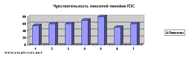

- For each pixel of the CCD line, a value is read when it is illuminated with a reference white light (and in more serious devices - and reading the "black level").
- The value is compared with a reference level (eg average).
- The difference between the output value and the reference level is stored for each pixel.
- Later, during scanning, this difference is compensated for for each pixel.
The AGC system is initialized every time the scanner system is initialized. You've probably noticed that when you turn on the machine, after a while, the scanner carriage begins to make progressive-return movements (crawl around the b / w strips). This is the initialization process for the AGC system. The system also takes into account the condition of the lamp (aging).
You also probably noticed that small MFPs equipped with a color scanner “light the lamp” in three colors in turn: red, blue and green. Then, only the original light turns white. This is done for better correction of the matrix sensitivity separately for RGB channels.
Halftone test (SHADING TEST) allows you to initiate this procedure at the request of the engineer and bring the correction values \u200b\u200bto real conditions.
Let's try to consider all this on a real, "combat" machine. Let's take a well-known and popular device as a basis. SAMSUNG SCX-4521 (Xerox Pe 220).
It should be noted that in our case CCD becomes CIS (Contact Image Sensor), but the essence of what is happening does not fundamentally change. Just as a light source, LED strips are used.
So:
The image signal from CIS has a level of about 1.2 V and is fed to the ADC section (SADC) of the apparatus controller (SADC). After SADC, the analog CIS signal will be converted to an 8-bit digital signal.
The image processor in SADC primarily uses the tone correction function, and then the gamma correction function. After that, the data is fed to the various modules in accordance with the operating mode. In Text mode, image data goes to the LAT module, in Photo mode, image data goes to the "Error Diffusion" module, and in PC-Scan mode, image data goes directly to a personal computer via DMA access.
Place several blank sheets of white paper on the exposure glass before testing. It goes without saying that the optics, b / w stripe and, in general, the scanner unit from the inside must be previously "licked"
- Select in TECH MODE
- Press the ENTER button to scan the image.
- After scanning, "CIS SHADING PROFILE" will be printed. An example of such a sheet is shown below. It does not have to be a copy of your result, but it is close in image.
- If the printed image is very different from the image shown in the figure, then the CIS is defective. Pay attention - at the bottom of the report sheet it says “Results: OK”. This means that the system has no serious complaints about the CIS module. Otherwise, error results will be given.
Example of profile printout:

Good luck to you!!
The materials of articles and lectures of teachers from St. Petersburg State University (LSU), St. Petersburg Electrotechnical University (LETI) and Axl are taken as a basis. Thanks to them.
Material prepared by V. Shelenberg
What is a CCD Matrix?
CCD / Charge-Coupled Device or CCD / Charge Coupled Device is an analog integrated circuit, which contains photosensitive photodiodes made of silicon or tin oxide. The principle of operation of this microcircuit is based on technology of devices with a charge-coupled device (CCD).
History of the CCD
For the first time, a charge-coupled device was used by George Smith and Willard Boyle at the Bell Laboratories of the largest US corporation AT&T Bell Labs in 1969. They conducted research in the field of video telephony and the so-called "semiconductor bubble memory".
Soon, miniature devices became widespread and began to be used as memory devices, in which the charge was placed in the input register of a microcircuit. Over time, the ability of a memory cell to receive a charge due to the photoelectric effect became the main goal of CCD devices.
A year later, in 1970, researchers from the same Laboratory were able to capture images using the simplest linear devices, which, in fact, was adopted by Sony engineers. This company is actively working in the field of CCD technologies to this day, investing huge financial investments in this area, in every possible way developing the production of CCD matrices for its video cameras. By the way, the CCD chip was installed on the tombstone of the head of Sony, Kazuo Iwama, who died in 1982. After all, it was he who stood at the origins of the beginning of the mass production of the CCD matrix.
The contribution of the inventors of the CCD matrix did not go unnoticed, so in 2006 Willard Boyle and George Smith received an award from the US National Academy of Engineering for their developments in this area, and in 2009 they were awarded the Nobel Prize in physics.
How the CCD works
The CCD matrix is \u200b\u200balmost entirely made of polysilicon, which was originally separated from the silicon substrate by a special membrane. When voltage is applied to the membrane by means of polysilicon gates, the electrical potentials located near the conductor electrodes change greatly.
Before exposure and applying a certain voltage to the electrodes, all charges that have formed earlier are discharged, and a transformation of all elements into an identical or original state is observed.
The combination of voltages on the electrodes creates a potential reserve or the so-called well, where electrons accumulate, which appeared in a certain pixel of the matrix during exposure under the influence of light rays. Depending on the intensity of the light flux, the volume of accumulated electrons in the potential well is also located, therefore, the larger it is, the higher the power of the final charge of a certain pixel will be.
After the end of exposure, successive changes in the supply voltage of the electrodes occur in each individual pixel, next to which the potential distribution is observed, as a result of which the charges move in a given direction - to the output pixels of the CCD matrix.
The composition of the elements of the CCD matrix
In general terms, the design of a CCD element can be represented as a p-type silicon substrate equipped with n-type semiconductor channels. Above these channels are electrodes made of polycrystalline silicon with an insulating silicon oxide membrane.
After applying an electric potential to these electrodes, a potential trap (well) appears in the weakened zone under the n-type channel. Its main task is to store electrons. A particle of light falling into silicon provokes the generation of electrons, which are attracted by a potential trap and remain in it. A large number of photons or bright light provides a powerful charge to the trap, after which it is necessary to calculate and enhance the value of the received charge, which experts call a photocurrent.
The process of reading the photocurrents of CCD elements is carried out with the so-called sequential shift registers, which convert a string of charges at the input to a series of pulses at the output. This stream of pulses is actually an analog signal that goes to the amplifier.
Thus, the line charges from CCD elements can be converted into an analog signal using a register. In practice, the sequential shift register in CCD matrices is performed using the same CCD elements built in one line. In this case, the operation of this device is based on the ability of charge-coupled devices to exchange charges of their potential traps. This process is carried out due to the presence of specialized transfer electrodes, which are placed between adjacent CCD-elements. At the moment the increased potential is applied to the nearest electrode, the charge passes under it from the potential well. At the same time, two to four transfer electrodes are usually located between CCD elements, the number of which determines the phase of the shift register, called two-phase, three-phase or four-phase.
The supply of different potentials to the transfer electrodes is synchronized in such a way that the transfer of the charges of potential traps of all CCD elements of the register is performed almost simultaneously. So in one "step" of transfer, CCD-elements move charges along the chain from right to left or from left to right. In this case, the extreme CCD element gives its charge to the amplifier, which is located at the register output. Thus, it becomes quite obvious that the serial shift register is a serial output and parallel input device.
After the process of reading absolutely all charges from the register is completed, it becomes possible to feed a new line to its input, then another, and so on. The result is a continuous analog signal based on a two-dimensional stream of photocurrents. Thereafter, the input parallel stream to the serial shift register is provided by a plurality of vertically oriented serial shift registers referred to as the parallel shift register. All this assembly in assembled form is precisely the device called today the CCD-matrix.
The matrix is \u200b\u200bthe main structural element of the camera and one of the key parameters taken into account by the user when choosing a camera. Matrices of modern digital cameras can be classified according to several signs, but the main and most common is even the division of matrices by charge sensing method, on: matrices CCD type and CMOS matrices. In this article we will consider the principles of operation, as well as the advantages and disadvantages of these two types of matrices, since they are commonly used in modern photography and video equipment.
CCD matrix
The matrix CCD also called CCD (Devices with Charging Connection). CCD the matrix is \u200b\u200ba rectangular plate of photosensitive elements (photodiodes) located on a semiconductor silicon crystal. The principle of its action is based on the line-by-line movement of charges that have accumulated in the gaps formed by photons in silicon atoms. That is, when colliding with a photodiode, a photon of light is absorbed and an electron is released (an internal photoelectric effect occurs). As a result, a charge is formed, which must be somehow stored for further processing. For this purpose, a semiconductor is embedded in the silicon substrate of the matrix, above which a transparent polycrystalline silicon electrode is located. And as a result of applying an electric potential to this electrode in the depletion zone under the semiconductor, a so-called potential well is formed, in which the charge received from photons is stored. When the electric charge is read from the matrix, the charges (stored in the potential wells) are transferred along the transfer electrodes to the edge of the matrix (serial shift register) and towards the amplifier, which amplifies the signal and transmits it to the analog-to-digital converter (ADC), from where the converted signal is sent to the processor, which processes the signal and saves the resulting image to the memory card .
For the manufacture of CCD matrices, polysilicon photodiodes are used. Such matrices are small in size and allow you to get high-quality photos when shooting with normal lighting.
Advantages of CCDs:
- The matrix design provides a high density of photocells (pixels) on the substrate;
- High efficiency (the ratio of registered photons to their total number is about 95%);
- High sensitivity;
- Good color rendering (with sufficient lighting).
Disadvantages of CCDs:
- High noise level at high ISO (at low ISO, noise level is moderate);
- Low operating speed in comparison with CMOS matrices;
- High power consumption;
- More complex technology for reading the signal, since many control microcircuits are needed;
- Manufacturing is more expensive than CMOS sensors.
CMOS matrix
Matrix CMOS, or CMOS sensor (Complementary Metal Oxide Semiconductors) uses active point sensors. Unlike CCDs, CMOSs \u200b\u200bcontain a separate transistor in each photosensitive element (pixel) so that charge conversion is performed directly in the pixel. The resulting charge can be read from each pixel individually, so there is no need for charge transfer (as it happens in CCDs). Pixels CMOS sensor integrates directly with an A / D converter or even a processor. This smart technology results in energy savings due to shorter process chains compared to CCDs, as well as cost savings due to a simpler design.

A brief principle of operation of the CMOS sensor: 1) Before shooting, a reset signal is sent to the reset transistor. 2) During exposure, light penetrates through the lens and filter onto the photodiode and as a result of photosynthesis, a charge accumulates in the potential well. 3) Read the value of the received voltage. 4) Data processing and image saving.
Advantages of CMOS Arrays:
- Low power consumption (especially in standby modes);
- High performance;
- Requires less production costs, due to the similarity of technology with the production of microcircuits;
- Unity of technology with other digital elements, which allows combining analog, digital and processing parts on one crystal (i.e., in addition to capturing light in a pixel, you can convert, process and clean the signal from noise).
- The ability to randomly access each pixel or group of pixels, which can reduce the size of the captured image and increase the read speed.
Disadvantages of CMOS sensors:
- The photodiode occupies a small pixel area, as a result, a low light sensitivity of the matrix is \u200b\u200bobtained, but in modern CMOS matrices this minus is practically eliminated;
- The presence of thermal noise from heating transistors inside the pixel during the readout process.
- Relatively large dimensions, fluorine equipment with this type of matrix is \u200b\u200bdistinguished by its large weight and dimensions.
In addition to the above types, there are also three-layer matrices, each layer of which is a CCD. The difference is that the cells can simultaneously perceive three colors, which are formed by dichroid prisms when a beam of light hits them. Then each beam is directed to a separate matrix. As a result, the brightness of blue, red and green colors is immediately detected on the photocell. Three-layer matrices are used in high-level video cameras, which have a special designation - 3CCD.
Summing up, I would like to note that with the development of technologies for the production of CCD and CMOS matrices, their characteristics also change, so it is more and more difficult to say which of the matrices is definitely better, but at the same time, CMOS matrices are becoming more and more popular in the production of SLR cameras. Based on the characteristic features of various types of matrices, you can get a clear idea why professional photographic equipment that provides high quality filming is rather bulky and heavy. This information must be remembered when choosing a camera - that is, take into account the physical dimensions of the matrix, and not the number of pixels.
The CCD was invented in 1969 by Willard Boyle and George Smith at AT&T Bell Labs. Laboratories worked on video telephony (eng. picture phone) and the development of "semiconductor bubble memory" (eng. semiconductor bubble memory). Charge coupled devices began life as memory devices in which one could only put a charge in the input register of the device. However, the ability of the device's memory element to receive a charge due to the photoelectric effect has made this application of CCD devices the main one.
General device and principle of operation
Before exposure, usually by applying a certain combination of voltages to the electrodes, all previously formed charges are released and all elements are brought into an identical state.
Further, the combination of voltages on the electrodes creates a potential well, in which electrons can accumulate, formed in a given pixel of the matrix as a result of exposure to light. The more intense the luminous flux during exposure, the more electrons accumulate in the potential well, respectively, the higher the final charge of a given pixel.
After exposure, successive changes in the voltage across the electrodes form in each pixel and next to it a potential distribution, which leads to a charge flow in a given direction to the output elements of the matrix.
Example of an n-pocket CCD sub-pixel
The pixel architecture is different for manufacturers.
Designations on the CCD subpixel diagram: 1 - photons of light that passed through the camera lens;
2 - ;
3 - R - red subpixel light filter, Bayer filter fragment;
4 - transparent electrode made of polycrystalline silicon or an alloy of indium and tin oxide;
5 - silicon oxide;
6 - n-type silicon channel: carrier generation zone - internal photoelectric effect zone;
7 - potential well zone (n-type pocket), where electrons are collected from the generation zone of charge carriers;
8 - p-type silicon substrate.
Buffering classification
Full-frame transfer matrices
The image formed by the lens hits the CCD matrix, that is, the light rays fall on the light-sensitive surface of the CCD elements, the task of which is to convert the photon energy into an electric charge. It happens in the following way.
For a photon falling on a CCD element, there are three scenarios - it will either "ricochet" from the surface, or be absorbed in the thickness of the semiconductor (matrix material), or "pierce through" its "working zone". Obviously, the developers are required to create such a sensor, in which the losses from "ricochet" and "lumbago right through" would be minimized. The same photons that were absorbed by the matrix form an electron-hole pair if there was an interaction with an atom of the crystal lattice of a semiconductor, or only an electron (or a hole) if the interaction was with atoms of donor or acceptor impurities, and both of these phenomena are called internal photoelectric effect ... Of course, the work of the sensor is not limited to the internal photoelectric effect - it is necessary to store the charge carriers "taken away" from the semiconductor in a special storage, and then read them.
CCD element
In general, the design of a CCD element looks like this: a p-type silicon substrate is equipped with channels of an n-type semiconductor. Above the channels, electrodes made of polycrystalline silicon with an insulating layer of silicon oxide are created. After applying an electric potential to such an electrode, a potential well is created in the depletion zone under the n-type channel, the purpose of which is to store electrons. A photon entering silicon leads to the generation of an electron, which is attracted by the potential well and remains in it. More photons (bright light) provide more charge to the well. Then you need to consider the value of this charge, also called photocurrent, and increase it.
The photocurrents of the CCD elements are read by so-called sequential shift registers, which convert a string of charges at the input to a series of pulses at the output. This series is an analog signal, which is then fed to the amplifier.
Thus, using the register, the charges of the line from the CCD elements can be converted into an analog signal. In fact, the serial shift register in CCDs is implemented using the same CCD elements concatenated into a string. The operation of such a device is based on the ability of CCD devices (this is what the abbreviation CCD stands for) to exchange charges of their potential wells. The exchange is carried out due to the presence of special transfer gates located between adjacent CCD elements. When an increased potential is applied to the nearest electrode, the charge "flows" under it from the potential well. Between the CCD elements, there can be two to four transfer electrodes, the "phase" of the shift register depends on their number, which can be called two-phase, three-phase or four-phase.
The supply of potentials to the transfer electrodes is synchronized in such a way that the movement of the charges of potential wells of all CCD elements of the register occurs simultaneously. And in one transfer cycle, the CCD elements "transfer along a chain" charges from left to right (or from right to left). Well, the CCD element that turned out to be the "extreme" gives its charge to the device located at the output of the register, that is, to the amplifier.
In general, a serial shift register is a parallel input and serial output device. Therefore, after reading all the charges from the register, it is possible to feed a new line to its input, then the next, and thus form a continuous analog signal based on a two-dimensional array of photocurrents. In turn, the input parallel stream for the sequential shift register (that is, the rows of a two-dimensional array of photocurrents) is provided by a set of vertically oriented sequential shift registers, which is called a parallel shift register, and the whole structure is just a device called a CCD matrix.
The "vertical" sequential shift registers that make up the parallel one are called CCD columns, and their operation is fully synchronized. The two-dimensional array of CCD photocurrents is simultaneously shifted down one row, and this happens only after the charges of the previous row from the sequential shift register located "at the very bottom" have gone to the amplifier. Until the serial register is freed, the parallel register has to be idle. Well, the CCD matrix itself for normal operation must necessarily be connected to a microcircuit (or a set of them), which supplies potentials to the electrodes of both serial and parallel shift registers, and also synchronizes the operation of both registers. In addition, a clock generator is needed.
Full-frame sensor
This type of sensor is the simplest from a constructive point of view and is called a full-frame CCD-matrix. In addition to the "strapping" microcircuits, this type of matrix also needs a mechanical shutter that blocks the luminous flux after the end of the exposure. It is impossible to start reading the charges until the shutter is completely closed - during the working cycle of the parallel shift register, extra electrons will be added to the photocurrent of each of its pixels, caused by the hit of photons on the open surface of the CCD matrix. This phenomenon is called "full-frame matrix smear".
Thus, the speed of reading a frame in such a scheme is limited by the speed of operation of both parallel and serial shift registers. It is also obvious that it is necessary to block the light flux coming from the lens until the reading process is complete, so the interval between exposures also depends on the reading speed.
Frame Buffered Matrices
There is an improved version of the full-frame matrix, in which the charges of the parallel register are not supplied line by line to the input of the serial register, but are "stored" in the buffer parallel register. This register is located under the main parallel shift register, the photocurrents are transferred line-by-line to the buffer register and from it are fed to the input of the serial shift register. The surface of the buffer register is covered with an opaque (usually metal) panel, and the whole system is called a frame - transfer CCD (frame - transfer CCD) matrix. Frame-buffered matrix In this scheme, potential pits of the main parallel shift register are "emptied" much faster, since when transferring lines to the buffer, there is no need to wait for a full cycle of the serial register for each line. Therefore, the interval between exposure is reduced, although the reading speed also decreases - the line has to "travel" twice the distance. Thus, the interval between exposures is reduced for only two frames, although the cost of the device due to the buffer register increases significantly. However, the most noticeable drawback of matrices with frame buffering is the extended "route" of photocurrents, which negatively affects the safety of their values. And in any case, a mechanical shutter should work between frames, so there is no need to talk about a continuous video signal.
Column-buffered matrices
A new type of matrix was developed especially for video equipment, in which the interval between exposures was minimized not for a couple of frames, but for a continuous stream. Of course, to ensure this continuity, it was necessary to provide for the abandonment of a mechanical shutter.
In fact, this scheme, called the interline CCD-matrix, is somewhat similar to frame-buffered systems - it also uses a buffer parallel shift register, the CCD elements of which are hidden under an opaque coating. However, this buffer is not located in a single block under the main parallel register - its columns are "shuffled" between the columns of the main register. As a result, there is a buffer column next to each column of the main register, and immediately after exposure, the photocurrents do not move “from top to bottom”, but “from left to right” (or “from right to left”), and in just one working cycle enter the buffer register, completely and completely freeing potential holes for the next exposure. The charges in the buffer register are read in the usual order through the sequential shift register, that is, "from top to bottom". Since the photocurrents are dumped into the buffer register in just one cycle, even in the absence of a mechanical shutter, nothing like "smearing" of the charge in a full-frame matrix is \u200b\u200bobserved. But the exposure time for each frame, in most cases, corresponds in duration to the interval spent on the full reading of the parallel buffer register. Thanks to all this, it becomes possible to create a video signal with a high frame rate - at least 30 frames per second. Column-buffered matrix Often in the domestic literature, column-buffered matrices are erroneously referred to as "interlaced". This is probably due to the fact that the English names "interline" (line buffering) and "interlaced" (interlaced scanning) sound very similar. In fact, when reading all lines in one clock cycle, we can speak of a progressive scan matrix, and when odd lines are read in the first clock cycle, and even lines are read in the second clock (or vice versa), we are talking about an interlace scan).
Sizes of camera matrices
| Designation | Width | Height | Diagonal | Area | Example | |
|---|---|---|---|---|---|---|
| Full frame, film type 135. |
1 - 1,01 | 35,8 - 36 | 23,8 - 24 | 43 - 43,3 | 852-864 | Canon EOS 5D, Canon EOS-1Ds (CMOS sensor) |
| APS-H | 1,26 - 1,28 | 28,1 - 28,7 | 18,7 - 19,1 | 33,8 - 34,5 | 525,5 - 548,2 | Canon EOS-1D Mark III (CMOS sensor) |
| 1,33 | 27 | 18 | 32,4 | 486 | Leica M8 | |
| APS-C,, 1.8 " | 1,44 - 1,74 | 20,7 - 25,1 | 13,8 - 16,7 | 24,9 - 30,1 | 285,7 - 419,2 | Pentax K10D |
| Foveon X3 | 1,74 | 20,7 | 13,8 | 24,9 | 285,7 | Sigma SD14 |
| 4/3 " | 1,92 - 2 | 17,3 - 18 | 13 −13,5 | 21,6 - 22,5 | 224,9 - 243 | Olympus E-330 |
| 1" | 2,7 | 12,8 | 9,6 | 16 | 122,9 | Sony ProMavica MVC-5000 |
| 2/3" | 3,93 | 8,8 | 6,6 | 11 | 58,1 | Pentax EI-2000 |
| 1/1,6" | ≈4 | 8 | 6 | 10 | 48 | Panasonic Lumix DMC-LX3 |
| 1/1,65" | ≈4 | Panasonic Lumix DMC-LX2 | ||||
| 1/1,7" | ≈4,5 | 7,6 | 5,7 | 9,5 | 43,3 | Canon PowerShot G10 |
| 1/1,8" | 4,84 | 7,176 | 5,319 | 8,9 | 38,2 | Casio EXILIM EX-F1 |
| 1/1,9" | ≈5 | Samsung Digimax V6 | ||||
| 1/2" | 5,41 | 6,4 | 4,8 | 8 | 30,7 | Sony DSC-D700 |
| 1/2,3" | ≈6 | 6,16 | 4,62 | 7,70 | 28,46 | Olympus SP-560 UZ |
| 1/2,35" | ≈6 | Pentax Optio V10 | ||||
| 1/2,4" | ≈6 | Fujifilm FinePix S8000fd | ||||
| 1/2,5" | 5,99 | 5,8 | 4,3 | 7,2 | 24,9 | Panasonic Lumix DMC-FZ8 |
| 1/2,6" | ≈6 | HP Photosmart M447 | ||||
| 1/2,7" | 6,56 | 5,27 | 3,96 | 6,6 | 20,9 | Olympus C-900 zoom |
| 1/2,8" | ≈7 | Canon DC40 | ||||
| 1/2,9" | ≈7 | Sony HDR-SR7E | ||||
| 1/3" | 7,21 | 4,8 | 3,6 | 6 | 17,3 | Canon PowerShot A460 |
| 1/3,1" | ≈7 | Sony HDR-SR12E | ||||
| 1/3,2" | 7,62 | 4,536 | 3,416 | 5,7 | 15,5 | Canon HF100 |
| 1/3,4" | ≈8 | Canon MVX35i | ||||
| 1/3,6" | 8,65 | 4 | 3 | 5 | 12 | JVC GR-DZ7 |
| 1/3,9" | ≈9 | Canon DC22 | ||||
| 1/4" | Canon XM2 | |||||
| 1/4,5" | Samsung VP-HMX10C | |||||
| 1/4,7" | Panasonic NV-GS500EE-S | |||||
| 1/5" | Sony DCR-SR80E | |||||
| 1/5,5" | JVC Everio GZ-HD7 | |||||
| 1/6" | 14,71 | 2,4 | 1,7 | 2,9 | 4,1 | Sony DCR-DVD308E |
| 1/8" | Sony DCR-SR45E |
Sizes of matrices of digital cinema cameras
| Designation | conformity format motion pictures |
Width |
|---|