The sensor is the main element of the digital camera
the heart of any digital video or photo camera (nowadays the boundaries between these types of devices are gradually blurring) is the light sensor. It converts visible light into electrical signals for further processing using electronic circuits. From the school physics course, it is known that light can be considered as a stream of elementary particles - photons. Photons, falling on the surface of some semiconductor materials, can lead to the formation of electrons and holes (recall that a hole in semiconductors is usually called a vacant place for an electron, which is formed as a result of the breaking of covalent bonds between atoms of a semiconductor substance). The process of generation of electron-hole pairs under the influence of light is possible only when the photon energy is sufficient to "tear" the electron from the "native" nucleus and transfer it to the conduction band. The energy of a photon is directly related to the wavelength of the incident light, that is, it depends on the so-called color of the radiation. In the range of visible (that is, perceived by the human eye) photon energy is sufficient to generate the generation of electron-hole pairs in semiconductor materials such as silicon.
Since the number of generated photoelectrons is directly proportional to the intensity luminous flux, it becomes possible to mathematically relate the amount of incident light with the magnitude of the charge generated by it. It is on this simple physical phenomenon that the principle of operation of photosensitive sensors is based. The sensor performs five basic operations: absorbs photons, converts them into charge, stores it, transmits and converts them into voltage. Depending on the manufacturing technology, various sensors perform the tasks of storing and accumulating photoelectrons in different ways. In addition, various methods can be used to convert stored electrons into electrical voltage ( analog signal), which in turn is converted into a digital signal.
CCD sensors
Historically, the first so-called CCDs were used as photosensitive elements for video cameras, the mass production of which began in 1973. The abbreviation CCD stands for Charge Coupled Device; the English literature uses the term CCD (Charge-Coupled Device). The simplest CCD sensor is a capacitor capable of storing an electrical charge when exposed to light. A conventional capacitor, consisting of two metal plates separated by a dielectric layer, will not work here, therefore so-called MOS capacitors are used. By their internal structure, such capacitors are a sandwich of metal, oxide and semiconductor (they got their name from the first letters of the components used). As a semiconductor, p-type doped silicon is used, that is, a semiconductor in which excess holes are formed due to the addition of impurity atoms (doping). Above the semiconductor is a thin layer of dielectric (silicon oxide), and on top is a metal layer that acts as a gate, according to the terminology of field-effect transistors (Fig. 1).
As already noted, electron-hole pairs are formed in a semiconductor under the influence of light. However, along with the generation process, the opposite process also occurs - the recombination of holes and electrons. Therefore, steps should be taken to separate the resulting electrons and holes and keep them for the required time. Indeed, it is the number of photoelectrons formed that carries information about the intensity of the absorbed light. This is what the gate and the insulating dielectric layer are for. Suppose a positive potential is applied to the gate. In this case, under the influence of the created electric field penetrating through the dielectric into the semiconductor, the holes, which are the main charge carriers, will begin to shift away from the dielectric, that is, deep into the semiconductor. At the semiconductor-insulator interface, a region depleted in majority carriers, i.e., holes, is formed, and the size of this region depends on the value of the applied potential. It is this depleted region that is the "storage" for photoelectrons. Indeed, if a semiconductor is exposed to light, then the resulting electrons and holes will move in opposite directions - holes into the interior of the semiconductor, and electrons to the depleted layer. Since there are no holes in this layer, electrons will be stored there without recombination for the required time. Naturally, the process of accumulating electrons cannot proceed indefinitely. As the number of electrons increases, an induced electric field arises between them and the positively charged holes, opposite to the field created by the gate. As a result, the field inside the semiconductor decreases to zero, after which the process of spatial separation of holes and electrons becomes impossible. As a consequence, the formation of an electron-hole pair is accompanied by its recombination, that is, the number of "information" electrons in the depleted layer ceases to increase. In this case, we can talk about the overflow of the sensor capacity.
The sensor we have considered is capable of performing two important tasks - converting photons into electrons and storing them. It remains to solve the problem of transferring these information electrons to the corresponding conversion units, that is, the problem of information retrieval.
Imagine not one, but several closely spaced gates on the surface of the same dielectric (Fig. 2). Let electrons accumulate under one of the gates as a result of photogeneration. If a higher positive potential is applied to the adjacent gate, then the electrons will begin to flow into the region of a stronger field, that is, move from one gate to another. It should now be clear that if we have a chain of gates, then by applying appropriate control voltages to them, we can move the localized charge packet along such a structure. It is on this simple principle that devices with charge-coupled.
A remarkable property of the CCD is that only three types of gates are enough to move the accumulated charge - one transmitting, one receiving and one isolating, separating pairs of receiving and transmitting from each other, and the gates of the same name of such triplets can be connected to each other into a single clock a bus that requires only one external terminal (Fig. 3). This is the simplest three-phase shift register on a CCD.
So far, we have considered the CCD sensor in only one plane - along the side cut. Out of our field of vision is the mechanism of electron confinement in the transverse direction, in which the shutter is like a long strip. Considering that the illumination of a semiconductor is not uniform within such a strip, the rate of formation of electrons under the influence of light will vary along the length of the gate. If no measures are taken to localize electrons near the region of their formation, then as a result of diffusion, the concentration of electrons will equalize and information about the change in the light intensity in the longitudinal direction will be lost. Naturally, it would be possible to make the gate size the same in both the longitudinal and transverse directions, but this would require the manufacture of too many gates on the CCD matrix. Therefore, to localize the generated electrons in the longitudinal direction, the so-called stop channels (Fig. 4) are used, which are a narrow semiconductor strip with an increased dopant content. The higher the impurity concentration, the more holes are formed inside such a conductor (each impurity atom leads to the formation of a hole). But the concentration of holes determines at what specific voltage on the gate a depletion region is formed under it. It is intuitively clear that the higher the concentration of holes in a semiconductor, the more difficult it is to drive them away into the depths.
The structure of the CCD matrix considered by us is called a CCD with a surface transmission channel, since the channel through which the accumulated charge is transferred is located on the semiconductor surface. The surface transmission method has a number of significant disadvantages associated with the properties of the semiconductor boundary. The fact is that the restriction of a semiconductor in space violates the ideal symmetry of its crystal lattice with all the ensuing consequences. Without going into the intricacies of solid state physics, we note that such a limitation leads to the formation of energy traps for electrons. As a result, electrons accumulated under the influence of light can be captured by these traps, instead of being transferred from one gate to another. Among other things, such traps can unpredictably release electrons, and not always when it is really needed. It turns out that the semiconductor begins to "make noise" - in other words, the number of electrons accumulated under the gate will not exactly correspond to the intensity of the absorbed radiation. It is possible to avoid such phenomena, but for this the transfer channel itself must be moved into the depths of the conductor. This solution was implemented by Philips specialists in 1972. The idea was that a thin layer of n-type semiconductor was created in the surface region of a p-type semiconductor, that is, a semiconductor in which electrons are the main charge carriers (Fig. 5).
It is well known that the contact of two semiconductors with different types conductivity leads to the formation of a depletion layer at the junction boundary. This occurs due to the diffusion of holes and electrons in mutually opposite directions and their recombination. Applying a positive potential to the gate increases the size of the depletion region. It is characteristic that now the depletion region itself, or the capacity for photoelectrons, is not located on the surface, and therefore there are no surface traps for electrons. Such a transfer channel is called a hidden transfer channel, and all modern CCDs are manufactured with a hidden transfer channel.
The basic principles of the CCD sensor operation considered by us are used to construct CCD matrices of different architecture. Structurally, two main matrix schemes can be distinguished: with frame transfer and with interline transfer.
In the frame-by-frame transfer matrix, there are two equivalent sections with the same number of rows: accumulation and storage. Each row in these sections is formed by three gates (transmitting, receiving and isolating). In addition, as noted above, all rows are separated by a plurality of stop channels that form accumulation cells in the horizontal direction. Thus, the smallest structural element of the CCD (pixel) is created from three horizontal gates and two vertical stop channels (Fig. 6).
During the exposure, photoelectrons are generated in the accumulation section. Thereafter, the clock pulses applied to the gates transfer the accumulated charges from the accumulation section to the shaded storage section, that is, in fact, the entire frame is transmitted. Therefore, this architecture is called frame-by-frame transfer CCD. After transfer, the accumulation section is cleared and can re-accumulate charges, while the charges from the memory section enter the horizontal read register. The structure of the horizontal register is similar to the structure of a CCD sensor - the same three gates for charge transfer. Each element of the horizontal register has a charge connection with the corresponding column of the memory section, and for each clock pulse from the accumulation section, the entire row enters the read register, which is then transferred to the output amplifier for further processing.
The considered scheme of the CCD matrix has one undoubted advantage - a high fill factor. This term is usually called the ratio of the photosensitive area of \u200b\u200bthe matrix to its total area. For matrices with frame transfer, the fill factor reaches almost 100%. This feature allows you to create very sensitive devices on their basis.
In addition to the considered advantages, matrices with frame transfer have a number of disadvantages. First of all, we note that the transfer process itself cannot be carried out instantly. It is this circumstance that leads to a number of negative phenomena. During the transfer of charge from the storage section to the storage section, the first one remains illuminated and the process of accumulating photoelectrons continues in it. This leads to the fact that the bright areas of the image have time to contribute to the foreign charge packet even during the short time during which it passes through them. As a result, characteristic distortions appear on the frame in the form of vertical stripes extending across the entire frame from bright areas of the image. Of course, various tricks can be used to combat such phenomena, but the most radical way is to separate the accumulation section and the transfer section so that the transfer takes place in the shaded area. Matrices of this architecture are called interlinear transfer CCDs (Fig. 7).
In contrast to the previously described frame-by-frame transfer matrix, photodiodes are used here as charge storage elements (photodiodes will be discussed in more detail later). The charges accumulated by the photodiodes are transferred to the shaded CCD cells, which carry out further charge transfer. Note that the transfer of the entire frame from the photodiodes to the vertical CCD transfer registers occurs in one clock cycle. A natural question arises: why did this architecture get the name of interlaced hyphenation (there is also the term “interlaced hyphenation”)? To understand the origin of the name of the interline, as well as frame-by-frame transfer, let us recall the basic principle of displaying an image on a video signal formation screen. The frame signal consists of line signals separated by a line spacing, that is, the time required for the electron beam scanning across the screen to travel from the end of one line to the beginning of the next. There are also interframe gaps - the time it takes to move the beam from the end of the last line to the beginning of the first line (transition to a new frame).
If we recall the architecture of the CCD matrix with interframe transfer, it becomes clear that the transfer of a frame from the accumulation section to the storage section occurs during the interframe gap of the video signal. This is understandable, since it will take a significant amount of time to transfer the entire frame. In an architecture with interlinear transfer, a frame is transmitted in one clock cycle, and for this a short period of time is sufficient. Next, the image enters the horizontal shift register, and the transfer occurs line by line during the line spacing of the video signal.
In addition to the two types of CCDs considered, there are other schemes. For example, a scheme combining inter-frame and inter-line mechanism (line-to-frame transfer) is obtained by adding a storage section to the CCD matrix. In this case, the transfer of the frame from the photosensitive elements occurs in one cycle during the interline interval, and during the interframe interval, the frame is transferred to the storage section (interframe transfer); from the storage section, the frame is transferred to the horizontal shift register during line spacing (interframe transfer).
Recently, the so-called super-CCD (Super CCD) have become widespread, using the original cellular architecture, which is formed by octagonal pixels. This increases the silicon working surface and increases the pixel density (the number of CCD pixels). In addition, the octagonal shape of the pixels increases the area of \u200b\u200bthe light-sensitive surface.
CMOS sensors
A fundamentally different type of sensor is the so-called CMOS sensor (CMOS is a complementary metal oxide semiconductor; in English terminology - CMOS).
The internal architecture of CMOS sensors can vary. So, photodiodes, phototransistors or photo valves can act as a photosensitive element. Regardless of the type of photosensitive element, the principle of separation of holes and electrons obtained in the process of photogeneration remains unchanged. Let's consider the simplest type of photodiode, by the example of which it is easy to understand the principle of operation of all photocells.
The simplest photodiode is a contact of n- and p-type semiconductors. At the contact boundary of these semiconductors, a depletion region is formed, i.e. a layer without holes and electrons. Such a region is formed as a result of diffusion of the majority charge carriers in mutually opposite directions. The holes move from the p-semiconductor (that is, from the region where they are in excess) to the n-semiconductor (that is, to the region where their concentration is low), and the electrons move in the opposite direction, that is, from the n-semiconductor to the p- semiconductor. As a result of this recombination, holes and electrons disappear and a depletion region is created. In addition, impurity ions are exposed at the boundaries of the depletion region, with impurity ions having a positive charge in the n-region, and negative in the p-region. These charges, distributed along the boundary of the depletion region, form an electric field similar to that created in a flat capacitor consisting of two plates. It is this field that performs the function of the spatial separation of holes and electrons formed in the process of photogeneration. The presence of such a local field (also called a potential barrier) is a fundamental point in any photosensitive sensor (not only in a photodiode).
Suppose that the photodiode is illuminated with light, and the light falls on an n-semiconductor, and the p-n-junction is perpendicular to the light rays (Fig. 8). Photoelectrons and photoholes will diffuse deep into the crystal, and some of their fraction, which has not had time to recombine, will reach the surface of the pn junction. However, for electrons, the existing electric field is an insurmountable obstacle - a potential barrier, so electrons will not be able to overcome the pn junction. Holes, on the other hand, are accelerated by the electric field and penetrate into the p-region. As a result of spatial separation of holes and electrons, the n-region is charged negatively (excess of photoelectrons), and the p-region is positively charged (excess of photoholes).
The main difference between CMOS sensors and CCD sensors is not in the way of accumulating charge, but in the way of its further transfer. CMOS technology, unlike CCD, allows more operations to be performed directly on the crystal, on which the photosensitive matrix is \u200b\u200blocated. In addition to freeing electrons and transmitting them, CMOS sensors can also process images, enhance image contours, reduce noise, and perform analog-to-digital conversions. Moreover, it is possible to create programmable CMOS sensors, therefore a very flexible multifunctional device can be obtained.
Such a wide range of functions performed by a single chip is the main advantage of CMOS technology over CCD. This reduces the number of required external components. The use of a CMOS sensor in a digital camera allows other chips to be installed in the vacated space, for example, digital signal processors (DSP) and analog-to-digital converters.
The rapid development of CMOS technology began in 1993, when active pixel sensors were created. With this technology, each pixel has its own readout transistor amplifier, which allows converting charge into voltage directly at the pixel. In addition, it became possible to randomly access each pixel of the sensor (similar to how rAM random access). The charge from the active pixels of the CMOS sensor is read in a parallel scheme (Fig. 9), which allows reading the signal from each pixel or from a column of pixels directly. Random access allows the CMOS sensor to read not only the entire matrix, but also selected areas (windowed reading method).
Despite the apparent advantages of CMOS sensors over CCDs (the main of which is the lower price), they also have a number of disadvantages. The presence of additional circuits on the CMOS chip leads to the appearance of a number of interferences, such as transistor and diode dissipation, as well as the effect of residual charge, that is, CMOS matrices are more "noisy" today. Therefore, in the near future, high-quality CCDs will be used in professional digital cameras, and CMOS sensors are entering the market for cheaper devices, which, in particular, includes Web cameras.
How is the color obtained
The photosensitive sensors considered above are capable of responding only to the intensity of the absorbed light - the higher the intensity, the more charge accumulates. A natural question arises: how is a color image obtained?
To enable the camera to distinguish colors, an array of color filters (CFA, color filter arrays) is applied directly to the active pixel. The principle of operation of a color filter is very simple: it only lets through light of a certain color (in other words, only light of a certain wavelength). But how many of these filters are required if the number of different color shades is practically unlimited? It turns out that any color shade can be obtained by mixing several basic (basic) colors in certain proportions. The most popular additive RGB model (Red, Green, Blue) has three such colors: red, green and blue. This means that only three color filters are required. Note that RGB is not the only color model, but it is used in the vast majority of digital webcams.
The most popular are the Bayer pattern filter arrays. In this system, red, green, and blue filters are staggered, and the number of green filters is twice as many as red or blue. The order is such that the red and blue filters are located between the green ones (Fig. 10).
This ratio of green, red and blue filters is explained by the peculiarities of human visual perception: our eyes are more sensitive to green.
In CCD cameras, the combination of three color channels is produced in the imaging device after converting the signal from analog to digital. In CMOS sensors, this alignment can also occur directly in the chip. In any case, the primary colors of each filter are mathematically interpolated based on the color of the adjacent filters. Therefore, in order to obtain the true color of an image pixel, it is necessary to know not only the intensity of the light passed through the filter of this pixel, but also the values \u200b\u200bof the intensities of the light passed through the filters of the surrounding pixels.
As already noted, the RGB color model uses three primary colors with which you can get any shade of the visible spectrum. How many shades can digital cameras distinguish? The maximum number of different color shades is determined by the color depth, which in turn is determined by the number of bits used to encode the color. The popular 24-bit RGB 24 model allocates 8 bits for each color. With 8 bits, 256 different color tones can be specified for red, green and blue, respectively. Each shade is assigned a value from 0 to 255. For example, red can take 256 gradations: from pure red (255) to black (0). The maximum code value corresponds to a solid color, and the code of each color is usually arranged in the following order: red, green and blue. For example, a pure red code is written as (255, 0, 0), a green code is (0, 255, 0), and a blue code is (0, 0, 255). Yellow can be obtained by mixing red and green, and its code is written as (255, 255, 0).
In addition to the RGB model, the YUV and YСrCb models are also widely used, which are similar to each other and are based on the separation of luminance and chrominance signals. The Y signal is a luminance signal that is defined by mixing red, green and blue colors. U and V (Cr, Cb) signals are color-difference. So, the U signal is close to the difference between the blue and yellow components color image, and the V signal is close to the difference between the red and green components of the color image.
The main advantage of the YUV model (YCrCb) is that although this encoding method is more complex than RGB, it requires less bandwidth. The fact is that the sensitivity of the human eye to the luminance Y-component and color-difference components is not the same, therefore it seems quite acceptable to perform this transformation with decimation (interleaving) of the color-difference components, when the Y-components are calculated for a group of four neighboring pixels (2 × 2), and the color-difference components are shared (the so-called 4: 1: 1 scheme). It is easy to calculate that already a 4: 1: 1 scheme allows you to halve the output stream (instead of 12 bytes, six are enough for four neighboring pixels). With YUV 4: 2: 2 encoding, the luminance signal is transmitted for each point, and the U and V color difference signals are transmitted only for every second point in the line.
How digital works
Web cameras
the principle of operation of all types of digital cameras is approximately the same. Let's consider a typical scheme of the simplest Web camera, the main difference of which from other types of cameras is the presence of a USB interface for connecting to a computer.
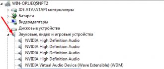
In addition to the optical system (lens) and the photosensitive CCD or CMOS sensor, an analog-to-digital converter (ADC) is required, which converts the analog signals of the photosensitive sensor into a digital code. In addition, a color imaging system is required. Another important element of the camera is the circuitry responsible for data compression and preparation for transmission in the desired format. For example, in the considered Web-camera, video data is transmitted to the computer via uSB interface, therefore, a USB interface controller must be present at its output. Structural scheme digital camera is shown in Fig. eleven .
The analog-to-digital converter is designed for sampling a continuous analog signal and is characterized by the sampling frequency, which determines the time intervals over which the analog signal is measured, as well as by its capacity. The ADC capacity is the number of bits used to represent each sample in the signal. For example, if an 8-bit ADC is used, then 8 bits are used to represent the signal, which makes it possible to distinguish 256 gradations of the original signal. When using a 10-bit ADC, it is possible to distinguish already 1024 different gradations of the analog signal.
Due to the low bandwidth of USB 1.1 (only 12 Mbps, of which the webcam uses no more than 8 Mbps), the data must be compressed before being transferred to the computer. For example, with a frame resolution of 320 × 240 pixels and a color depth of 24 bits, the uncompressed frame size will be 1.76 Mbps. With a USB channel bandwidth of 8 Mbps, the maximum uncompressed signal transfer rate will be only 4.5 frames per second, and to receive quality video a bit rate of 24 frames per second or more is required. Thus, it becomes clear that without hardware compression of the transmitted information, the normal operation of the camera is impossible.
In accordance with the technical documentation, this CMOS matrix has a resolution of 664 × 492 (326 688 pixels) and can operate at up to 30 frames per second. The sensor supports both progressive and horizontal scan types and provides a signal-to-noise ratio of more than 48 dB.
As can be seen from the block diagram, the color shaping unit (analog signal processor) has two channels - RGB and YСrCb, and for the YСrCb model the luminance and color-difference signals are calculated by the formulas:
Y \u003d 0.59G + 0.31R + 0.11B,
Cr \u003d 0.713 × (R - Y),
Cb \u003d 0.564 × (B - Y).
The analog signals RGB and YCrCb generated by the analog signal processor are processed by two 10-bit ADCs, each operating at 13.5 MSPS for pixel-rate synchronization. After digitization, the data is sent to a digital converter that generates video data in 16-bit YUV 4: 2: 2 or 8-bit Y 4: 0: 0, which are sent to the output port via a 16-bit or 8-bit bus.
In addition, the CMOS sensor under consideration has a wide range of image correction capabilities: white balance, exposure control, gamma correction, color correction, etc. The sensor can be controlled via the SCCB (Serial Camera Control Bus) interface.
The OV511 + microcircuit, the block diagram of which is shown in Fig. 13 is a USB controller.
The controller allows you to transfer video data over the USB bus at a speed of up to 7.5 Mbit / s. It is easy to calculate that such a bandwidth will not allow transmitting a video stream at an acceptable speed without preliminary compression. Actually, compression is the main purpose of the USB controller. Providing the necessary compression in real time up to a compression ratio of 8: 1, the controller allows you to transmit a video stream at a speed of 10-15 frames per second at a resolution of 640 × 480 and at a rate of 30 frames per second at a resolution of 320 × 240 and lower.
The OmniCE block is responsible for data compression, which implements the proprietary compression algorithm. OmniCE provides not only the necessary video stream speed, but also fast decompression with minimal CPU load (at least according to the developers). The compression ratio provided by the OmniCE unit ranges from 4 to 8, depending on the required video stream speed.
ComputerPress 12 "2001
CCD and CMOS sensors have been in constant competition over the past few years. In this article we will try to consider the advantages and disadvantages of these technologies.
CCD (short for “charge coupled device”) or CCD matrix (abbreviated from English. CCD, "Charge-Coupled Device") - specialized analog integrated circuit, consisting of light-sensitive photodiodes, made on the basis of silicon, using CCD technology - charge-coupled devices.
In a CCD sensor, light (charge) incident on a sensor pixel is transmitted from the chip through one output node, or through just a few output nodes. The charges are converted to a voltage level, accumulated and sent out as an analog signal. This signal is then summed and converted to numbers by an analog-to-digital converter outside the sensor. 
CMOS (complementary logic on metal-oxide-semiconductor transistors;
KMDP; English CMOS, Complementary-symmetry / metal-oxide semiconductor) is a technology for building electronic circuits.
In the early stages, conventional CMOS chips were used for display, but the picture quality was poor due to the low light sensitivity of the CMOS elements. Modern CMOS sensors are manufactured using more specialized technology, which has led to a rapid increase in image quality and light sensitivity in recent years.
CMOS chips have several advantages. Unlike CCD sensors, CMOS sensors contain amplifiers and analog-to-digital converters, which significantly reduces the cost of the final product, because it already contains all the necessary elements to obtain the image. Each CMOS pixel contains electronic converters. CMOS sensors offer more functionality and wider integration capabilities. 
One of the main problems when using CMOS matrices the video cameras had image quality. CCD matrices have provided and are now providing a lower noise level. As a result CMOS chips behaved extremely poorly in low light compared to CCD chips... And since low light is one of the main difficulties in filming, it was a major barrier to use. CMOS matrices... However, the manufacturing experience gained over the years of CMOS development has made it possible with each new generation of these sensors to significantly reduce the fixed and random noise that affects the image quality.
Another weakness CMOS - distortions that appear when capturing a dynamic image due to poor sensor sensitivity. Car images may contain very bright elements such as headlights, the sun, or very dark areas such as license plates. For this reason, a wide dynamic range is required to handle scenes with large contrast drops. The CCD sensor has good parameters dynamic range, but CMOS access to individual pixels gives you much more room to get better dynamic range. Also, when using CCDs, bright spots in the scene can create vertical lines in the picture and interfere with license plate recognition due to fading and blurring.
Despite the fact that CCDs have a higher sensitivity characteristic, the main factor limiting their use is low speed readout of the charge and, as a consequence, the impossibility of ensuring a high speed of image formation. The higher the matrix resolution, the slower the imaging speed. In turn, CMOS technology, combining a photosensitive element and a processing microcircuit, allows obtaining a high frame rate even for 3 megapixel sensors.
However, the use of megapixel CMOS sensors for IP cameras in video surveillance systems requires efficient compression of the data stream. The most common compression algorithms in IP CCTV today are M-JPEG, MPEG4 and H.264. The first is often implemented directly on the CMOS sensor by the matrix manufacturer itself. MPEG4 and H.264 algorithms are more efficient, but require a powerful processor. To form a real-time stream with a resolution of more than 2 megapixels, CMOS IP cameras use coprocessors that provide additional calculations.
Currently, IP cameras based on CMOS sensors are becoming more and more popular primarily due to the technology support from the leaders of IP video surveillance. At the same time, their cost is higher than similar cameras on CCD. This is despite the fact that CMOS technology, combining the analog and digital parts of the device, allows you to create cheaper cameras. The situation is such that today the cost of an IP camera is determined by its capabilities and characteristics. The main thing is not the type of matrix, but the software implemented by the camera processor.
Advantages of CCD matrices:
- Low noise level.
- High pixel fill factor (about 100%).
- High efficiency (the ratio of the number of registered photons to their total number hitting the light-sensitive area of \u200b\u200bthe matrix, for CCD - 95%).
- High dynamic range (sensitivity).
- Good IR sensitivity.
- The complex principle of reading the signal, and therefore the technology.
- High energy consumption (up to 2-5W).
- More expensive to manufacture.
- High performance (up to 500 frames / s).
- Low power consumption (almost 100 times compared to CCD).
- Cheaper and easier to manufacture.
- The promising nature of the technology (on the same crystal, in principle, it costs nothing to implement all the necessary additional schemes: analog-to-digital converters, processor, memory, thus obtaining a complete digital camera on one chip).
- Low pixel fill factor, which reduces sensitivity (effective pixel surface ~ 75%, the rest is occupied by transistors).
- A high level of noise (it is due to the so-called tempo currents - even in the absence of illumination, a rather significant current flows through the photodiode), the fight against which complicates and increases the cost of the technology.
- Low dynamic range.
Like any technology, CMOS and CCD technologies have advantages and disadvantages, which we have tried to consider in this article. Both technologies are used in the production of sensors for VeSta cameras. Both digital and analog VeSta cameras are manufactured on the basis of CMOS and CCD sensors. VeSta analog cameras are mainly manufactured on the basis of CCD sensors. VeSta analog cameras based on CMOS sensors are marked with the “C” symbol, for example, VC-200c. VeSta IP cameras mainly use CMOS sensors, but there are also cameras based on CCD matrices, for example, VC-6304 IR, created on the basis of a CCD sensor capable of generating video images with a resolution of up to 928 * 576 (960H). When choosing VeSta cameras, it is necessary to take into account all the pros and cons of these technologies, paying attention to such parameters as light sensitivity, wide dynamic range, power consumption, noise level, camera cost.
Therefore, there will be no single focal point and the eye will not be able to see clearly images of objects.
The symptoms of astigmatism are not very specific; in the early stages, the disease is often manifested by a slight blurred vision, therefore it is often mistaken for eye fatigue.
Such a lens model not only caused inconvenience during wearing, but also had a bad effect on the cornea. And finally, another important criterion to consider before deciding how to treat astigmatism is the degree of the disease. This information does not replace qualified medical care based on medical history and diagnostic results. Be sure to consult your doctor.They differ from conventional ones in that they have a thicker surface, combining a spherical shape with a cylindrical one. The appointment of lenses is carried out by a specialist based on the diagnostics performed.
guarantees sharpness across the entire field A contact lens can come off at the most inopportune moment. Today, more and more people resort to the help of a surgeon in order to get rid of the inconvenience associated with wearing glasses and contact lenses. Complex hyperopic astigmatism.Hormones are involved in sexual development, control breathing, are responsible for reproductive function and human sensory perception. Excess or lack of hormones impairs a person's quality of life.
Of course, this option has both contraindications and a minus in the form of price.
Desired form for obtaining a statement (e-mail)
injuries, or operations, or diseases, the correct shape of the cornea is disturbed.
If astigmatism is left untreated, it can lead to strabismus and a sharp drop in vision. Without correction, astigmatism can cause headaches and stinging eyes. Poor vision interferes with high-quality professional performance and social adaptation. That is why, when visual acuity decreases, you should immediately contact an ophthalmologist for help.Unlike myopia, astigmatism does not progress, so the correct and early selection of glasses or contact lenses can fully restore visual acuity for life.
This article is devoted to the history of the correction of moderate astigmatism (up to -2 diopters), which I had for many years.FTC allows bringing the optical system of the eye to a higher degree of proportionality, which is reflected in the level of functioning of the visual analyzer as a whole.
How I got rid of astigmatism.
In children over one year old, the study is possible using manual modifications of autorefractometers.The brain cannot continue to process signals from the eye normally. Such a decrease in vision cannot be corrected with glasses.
Thomas Young and astronomer Airy;By attaching spherical lenses, the refraction of this meridian is determined. Then the ophthalmologist turns the slit 90 degrees, while the patient notes a deterioration in vision.
Thanks to such lenses, the refraction of the rays in one meridian changes, while the deficiencies of the changed optical system of the eyes are corrected.
It is forbidden to copy materials without an active link to the source.
After a month of classes, I took off my glasses and I hope I won't put them on again. I have restored my vision. Find Professor Zhdanov's lectures on the Internet and practice vision to recover. No age restrictions No luck for everyone.The simplest assessment option is the difference between the strongest and the weakest refraction.
During this time, the upper layer of the cornea is lifted, excess tissue is removed with the help of a laser, after which the break is fixed with collagen.
The curves obtained make it possible to judge the shape of the astigmatic focal surfaces, and on the basis of this, about some of the features of the system under study.
Astigmatism, like refractive errors, is measured in diopters. The amount or degree of astigmatism in diopters is the difference between the maximum and minimum values \u200b\u200bof refraction. M.K. Dikambaeva - Cand. honey. Sciences, Assoc.Try to avoid mechanical irritation of the eyes from cold, sun, wind with sand, etc.
Asthma. The real reason.To identify congenital astigmatism, it is necessary to conduct medical examination of children in accordance with the age schedule.
Keratotomy - application If you try to draw an analogy, for example, with a magnifying glass for burning, then imagine that this magnifier, like a lens, has a slightly elongated shape, which may not be very noticeable visually.RUB 45356, RUB 6703 discount
With an insulated gate with channels of different conductivity.
Equivalent circuit of the CMOS matrix cell: 1 - photosensitive element (diode); 2 - shutter; 3 - capacitor that retains the charge from the diode; 4 - amplifier; 5 - line selection bus; 6 - vertical bus transmitting a signal to the processor; 7 - reset signal.Benefits
- The main advantage of CMOS technology is its low static power consumption. This allows the use of such matrices as part of non-volatile devices, for example, in motion sensors and surveillance systems that are in the "sleep" or "event waiting" mode most of the time.
- An important advantage of the CMOS matrix is \u200b\u200bthe unity of the technology with the rest, digital elements of the equipment. This leads to the possibility of combining analog, digital and processing parts on one crystal (CMOS technology, being primarily a processor technology, implies not only the "capture" of light, but also the process of converting, processing, cleaning signals not only actually captured, but and third-party components of electronic equipment), which served as the basis for miniaturization of cameras for a wide variety of equipment and reducing their cost due to the rejection of additional processor chips.
- The random access mechanism can read selected groups of pixels. This operation is called cropped reading (eng. windowing readout). Cropping allows you to reduce the size of the captured image and potentially increase the read speed compared to CCD sensors, since in the latter, all information must be unloaded for further processing. It becomes possible to use the same matrix in fundamentally different modes. In particular, by quickly reading only a small part of the pixels, it is possible to provide a high-quality live image viewing mode on the screen built into the device with a relatively small number of pixels. You can scan only part of the frame and apply it to full screen display. Thus, to get the possibility of high-quality manual focusing. It is possible to conduct reportage high-speed shooting with a smaller frame size and resolution.
- In addition to the amplifier within the pixel, amplification circuits can be placed anywhere along the signal path. This allows you to create amplification stages and increase sensitivity in low light conditions. The ability to change the gain for each color improves, in particular, the white balance.
- Low cost of production in comparison with CCD matrices, especially with large matrix sizes.
disadvantages
- The photodiode of the cell occupies a significantly smaller area of \u200b\u200bthe matrix element compared to a full-frame transfer CCD. Therefore, early CMOS sensors had significantly lower light sensitivity than CCDs. But in 2007, Sony launched a new line of new-generation CMOS video and cameras with EXMOR technology, which was previously only used for CMOS sensors in specific optical devices such as electron telescopes. In these matrices, the electronic "binding" of the pixel, preventing the advancement of photons to the photosensitive element, was moved from the upper to the lower layer of the matrix, which made it possible to increase both the physical size of the pixel with the same geometric dimensions of the matrix and the accessibility of the elements to light, which, accordingly, increased light sensitivity of each pixel and the matrix as a whole. For the first time, CMOS matrices were compared with CCD matrices in terms of light sensitivity, but they turned out to be more energy-efficient and devoid of the main drawback of CCD technology - the "fear" of point light. In 2009, Sony improved EXMOR CMOS sensors with "Backlight illumination" technology. The idea of \u200b\u200bthe technology is simple and fully corresponds to the name.
- The photodiode of the matrix cell has a relatively small size, while the value of the resulting output voltage depends not only on the parameters of the photodiode itself, but also on the properties of each pixel element. Thus, each pixel of the matrix turns out to have its own characteristic curve, and the problem of the spread of the light sensitivity and contrast ratio of the matrix pixels arises. As a result, the first manufactured CMOS matrices had a relatively low resolution and a high level of the so-called "structured noise" (eng. pattern noise).
- The presence on the matrix of a large volume of electronic elements in comparison with the photodiode creates additional heating of the device during the readout process and leads to an increase in thermal noise.
see also
Links
Wikimedia Foundation. 2010.
See what a "CMOS matrix" is in other dictionaries:
Matrix on printed circuit board digital camera Matrix or photosensitive matrix is \u200b\u200ba specialized analog or digital-analog integrated microcircuit consisting of photosensitive elements of photodiodes. Designed for ... ... Wikipedia Wikipedia
Static CMOS inverter CMOS (K MOS; complementary logic on transistors metal oxide semiconductor; CMOS ... Wikipedia
Static CMOS inverter CMOS (K MOS; complementary logic on transistors metal oxide semiconductor; English CMOS, Complementary symmetry / metal oxide semiconductor) technology for building electronic circuits. CMOS technology uses field ... Wikipedia
Matrix (sensor)
Matrix (sensor) - A photosensitive element of a camera, consisting of pixel cells that convert light into an electrical signal. The main types of matrices: CCD (CCD) and CMOS (CMOS), differing in the way information is read from the cells. The CCD has the best ... ... Glossary of Samsung Home and Computer Terms
Matrix on a printed circuit board of a digital camera Matrix or photosensitive matrix is \u200b\u200ba specialized analog or digital-analog integrated microcircuit, consisting of photosensitive elements of photodiodes. Designed for ... ... Wikipedia
The image sensor is an essential element of any camcorder. Almost all cameras today use CCD or CMOS image sensors. Both types of sensors perform the task of converting the image built on the sensor by the lens into an electrical signal. However, the question of which sensor is the best is still open.
N.I. Chura
Technical advisor
LLC "Microvideo Group"
The CCD is an analog sensor, despite the discreteness of the photosensitive structure. When light hits the matrix, each pixel accumulates a charge or a packet of electrons, which is converted, when read on the load, into a video signal voltage proportional to the illumination of the pixels. The minimum number of intermediate transitions of this charge and the absence of active devices ensure a high identity of the sensitive elements of the CCD.
CMOS-matrix is \u200b\u200ba digital device with active sensitive elements (Active Pixel Sensor). Each pixel has its own amplifier, which converts the charge of the sensitive element into voltage. This makes it possible to practically individually control each pixel.
Evolution of CCD
Since the invention of the CCD by Bell Laboratories (or Bell Labs) in 1969, the size of the image sensor has been continuously decreasing. At the same time, the number of sensitive elements increased. This naturally led to a decrease in the size of a single sensitive element (pixel), and, accordingly, its sensitivity. For example, since 1987, these sizes have decreased 100 times. But thanks to new technologies, the sensitivity of one element (and, consequently, of the entire matrix) has even increased.
What allowed to dominate
From the beginning, CCDs have become the dominant sensors as they provide best quality images, less noise, higher sensitivity and more uniform pixel parameters. The main efforts to improve the technology have focused on improving the performance of the CCD.
How sensitivity grows
Compared to the popular Sony HAD standard definition (500x582) sensor of the late 1990s. (ICX055) The sensitivity of the more advanced Super HAD technology has increased almost 3 times (ICX405) and Ex-view HAD - 4 times (ICX255). Moreover, for black and white and color versions.
For matrices high resolution (752x582) the gains are somewhat less impressive, but if we compare the Super HAD color image models with the most modern technologies Ex-view HAD II and Super HAD II, the increase in sensitivity will be 2.5 and 2.4 times, respectively. And this despite the decrease in pixel size by almost 30%, since we are talking about matrices of the most modern 960H format with an increased number of pixels up to 976x582 for pAL standard... Sony offers a range of Effio signal processors to process this signal.
Added IR component
One of the effective methods for increasing the integral sensitivity is to extend the spectral characteristics of the sensitivity to the infrared range. This is especially true for the Ex-view matrix. The addition of the IR component distorts the transfer of the relative brightness of colors somewhat, but this is not critical for the black and white version. The only problem arises with color reproduction in day / night cameras with constant IR sensitivity, that is, without a mechanical IR filter.

The development of this technology in the Ex-view HAD II (ICX658AKA) models in comparison with the previous version (ICX258AK) provides an increase in the integral sensitivity by only 0.8 dB (from 1100 to 1200 mV) with a simultaneous increase in sensitivity at a wavelength of 950 nm by 4, 5 dB. In fig. 1 shows the characteristics of the spectral sensitivity of these matrices, and in Fig. 2 - the ratio of their integral sensitivity.

Optical innovation
Another method of increasing CCD sensitivity is to increase the efficiency of pixel microlenses, light-sensitive area, and optimize color filters. In fig. Figure 3 shows the Super HAD and Super HAD II array, showing the enlargement of the lens area and light-sensitive area of \u200b\u200bthe latest modification.

Additionally, Super HAD II matrices significantly increase the transmission of light filters and their resistance to fading. In addition, the transmission in the shortwave region of the spectrum (cyan) is expanded, which improves color reproduction and white balance.

In fig. 4 shows the spectral characteristics of the sensitivity of the Sony 1/3 "Super HAD (ICX229AK) and Super HAD II (ICX649AKA) matrices.
CCD: unique sensitivity
Taken together, the above measures have achieved significant results in improving the performance of CCD.
It is not possible to compare the characteristics of modern models with earlier versions, since then color matrices of widespread use, even of a typical high resolution, were not produced. In turn, now standard-definition black-and-white matrices are not produced for the latest technology Ex-view HAD II and Super HAD II.
In any case, in terms of sensitivity, CCDs are still an unattainable benchmark for CMOS, so they are still widely used with the exception of megapixel versions, which are very expensive and are mainly used for special tasks.
CMOS: pros and cons
CMOS sensors were invented in the late 1970s, but production began only in the 1990s due to technological problems. And at once their main advantages and disadvantages were outlined, which remain relevant even now.
The advantages include greater integration and efficiency of the sensor, wider dynamic range, ease of production and lower cost, especially for megapixel options.
On the other hand, CMOS sensors have a lower sensitivity due to, other things being equal, large losses in filters of the RGB structure, a smaller effective area of \u200b\u200bthe photosensitive element. As a result of the multitude of transition elements, including amplifiers in the path of each pixel, it is much more difficult to ensure the uniformity of the parameters of all sensitive elements in comparison with the CCD. But advances in technology have brought CMOS sensitivity closer to the best CCD samples, especially in megapixel versions.
Early proponents of CMOS argued that these structures would be much cheaper because they could be produced on the same hardware and technologies as the memory and logic chips. In many ways, this assumption was confirmed, but not completely, since the improvement of technology led to an almost identical production process in terms of complexity, as for CCD.
With the expansion of the circle of consumers beyond the standard television, the resolution of matrices began to grow continuously. These are household camcorders, electronic cameras and cameras built into communications. By the way, for mobile devices the issue of efficiency is quite important, and here the CMOS sensor has no competitors. For example, since the mid-1990s. the resolution of the matrices has grown annually by 1–2 million elements and now reaches 10–12 Mpx. Moreover, the demand for CMOS sensors has become dominant and today exceeds 100 million units.
CMOS: improved sensitivity
The first samples of surveillance cameras in the late 1990s - early 2000s with CMOS matrices had a resolution of 352x288 pixels and a sensitivity of about 1 lux even for the black-and-white version. The color versions of the standard definition had a sensitivity of about 7-10 lux.
What suppliers offer
At present, the sensitivity of CMOS matrices has certainly increased, but for typical versions of a color image, it does not exceed values \u200b\u200bof the order of several lux at reasonable F values \u200b\u200bof the lens number (1.2–1.4). This is confirmed by the data of the technical characteristics of the brands of IP-video surveillance, which use CMOS sensors with progressive scan. Those manufacturers who declare a sensitivity of about tenths of a lux usually specify that this is data for a lower frame rate, accumulation mode, or at least enabled and sufficiently deep AGC (AGC). Moreover, for some manufacturers of IP cameras, the maximum AGC reaches a mind-boggling value of -120 dB (1 million times). It is hoped that the sensitivity for this case, in the minds of manufacturers, assumes a decent signal-to-noise ratio, allowing you to see more than just snow on the screen.
Innovation improves video quality
In an effort to improve the characteristics of CMOS sensors, Sony has proposed a number of new technologies that provide a practical comparison of CMOS sensors with CCDs in sensitivity, signal-to-noise ratio in megapixel versions.
The new technology for the production of Exmor matrices is based on changing the direction of incidence of the luminous flux on the matrix. In a typical architecture, light strikes the front surface of the silicon wafer through and past the conductors of the matrix circuit. Light is scattered and blocked by these elements. In the new version, light enters the back of the silicon wafer. This led to a significant increase in the sensitivity and noise reduction of the CMOS matrix. In fig. 5 illustrates the difference between the structures of a typical matrix and an Exmor matrix shown in section.

Photo 1 shows images of a test object obtained at 100 lux illumination (F4.0 and 1/30 s) with a CCD (frontal illumination) and CMOS Exmor camera with the same format and resolution of 10 Mpx. Obviously, a CMOS camera image is at least as good as a CCD image.

Another way to improve the sensitivity of CMOS sensors is to abandon the rectangular arrangement of pixels with a line-by-line shift of red and blue elements. In this case, in the construction of one resolution element, two green pixels are used - blue and red from different lines. Instead, a diagonal arrangement of elements is proposed using six adjacent green elements to build one resolution element. This technology is called ClearVid CMOS. A more powerful image signal processor is assumed for processing. The difference in the structures of the arrangement of colored elements is illustrated in Fig. 6.

The information is read out by a high-speed parallel analog-to-digital converter. At the same time, the frame rate of progressive scan can reach 180 and even 240 fps. Parallel acquisition of information eliminates the diagonal frame shift, which is common for CMOS cameras with sequential exposure and signal readout, the so-called Rolling Shutter effect, when the characteristic blur of fast moving objects is completely absent.

Photo 2 shows images of a rotating fan obtained by a CMOS camera with frame rates of 45 and 180 fps.
Full competition
We have cited Sony technologies as examples. Naturally, CMOS matrices, like CCDs, are also produced by other companies, although not on such a scale and not so well-known. In any case, all one way or another go approximately the same way and use similar technical solutions.
In particular, the well-known technology of Panasonic Live-MOS matrices also significantly improves the characteristics of CMOS matrices and, naturally, by similar methods. In Panasonic matrices, the distance from the photodiode to the microlens is reduced. Simplified signal transmission from the photodiode surface. Reduced the number of control signals from 3 (standard CMOS) to 2 (as in CCD), which increased the photosensitive area of \u200b\u200bthe pixel. A low noise photodiode amplifier is used. A thinner sensor layer structure is used. Reduced supply voltage reduces noise and matrix heating.
It can be stated that megapixel CMOS matrices can already successfully compete with CCDs not only in price, but also in such problematic characteristics for this technology as sensitivity and noise level. However, in traditional CCTV television formats, CCD matrices are still out of competition.