The main classification parameters of the memory
| Parameter | Designation | Definition |
| Information capacity | N | The number of bits of memory in the storage device |
| Number of words and memory | NS | Number of word addresses in the memory drive |
| Bit depth | T | The number of bits in the memory drive |
| Output branching ratio | K p | The number of unit loads (inputs of other ICs) that can be simultaneously connected to the memory output |
| Number of reprogramming cycles | Ncy | The number of write-erase cycles at which the memory remains operational |
| Power consumption | p CC | Power consumption of the charger in the set operating mode |
| Power consumption in storage mode | p CCS | The power consumed by the memory when storing information in the non-select mode |
| Information storage time | t SG | The time interval during which the memory stores information in a given mode |
Static parameters 3U
An important advantage of ROM over RAM is the retention of information when the power is turned off. The cost of a bit of information stored in ROM can be almost an order of magnitude lower than in RAM. Permanent storage devices can be implemented based on various physical principles.
Currently, the following types of ROM are used:
MASK ROMS are programmed by their manufacturer, who, according to the information prepared by the user, makes photo templates, with the help of which he enters this information into the ROM crystal during the production process. This method is the cheapest and is intended for large-scale production of ROMs.
Masked ROMs are built on the basis of diodes, bipolar and MOS transistors. In diode ROM, diodes are included in those matrix intersections that correspond to the entry "1", and are absent in the places where the "0" should be written. The external control circuits of diode ROMs are very simple. Since the diode array is a galvanically coupled element, the output signals have the same shape as the input signals. Permanent memory devices based on MIS transistors are somewhat easier to manufacture than bipolar ones.
Masked ROMs are characterized by high reliability, but it is impossible to change the information in the ROM without making a new IC, which is especially inconvenient at the stage of developing the system programs.
USER PROGRAMMABLE ROMs are more versatile and therefore more expensive. They are matrices of bipolar devices with fusible jumpers (their simplified diagram is shown in Fig.17.7), the connections of which with the address and bit buses are destroyed when the code is entered on special PROGRAMMERS... These devices generate voltages necessary and sufficient to burn through the fuse links in the selected memory elements of the ROM.
In fig. ... fusible jumpers PP are shown in the form of fuses included in the emitters of multi-emitter transistors VTo ... VTp. Programmable elements are included between the emitters of the matrix transistors and the bit lines. The presence of a jumper corresponds to a logical 0 at the output of the readout amplifier, and the absence of a jumper corresponds to a logical unit. The process of writing information to the circuit is the selective destruction of fuse links by the current provided by the programming device
ONE TIME PROGRAMMABLE ROM (EPROM) the drive is performed on the basis of cells. Permanent memory devices of this type allow only one-time recording of information in a cell. When programming, "these fusible jumpers made of nichrome or other refractory material are burned out using a special programming device. Burning of jumpers in programming mode is performed by a series of pulses according to a special program.
To increase the reliability of the ROM operation, the programming technique provides for the delivery of a series of 40, .. 100 pulses after fixing the moment of burning the jumper, as well as mandatory thermal training of the programmed ROM at a temperature (about 100 ° C).
More reliable are microcircuits with polycrystalline silicon jumpers, in which the process of irreversible transition of polysilicon from a conducting state to a non-conducting state occurs under the action of heating caused by the flow of current.
The programming mode support circuits are usually located on the chip itself, and the programming process proceeds as follows.
1) The address of the selected cell is supplied to the address inputs.
2) The supply voltage of the microcircuit + U rises to the programming voltage +10 V required to create a current, I ³ 400 mA sufficient to melt the jumper.
3) A voltage of +15 V with a current of no more than 100 mA is supplied to the programming input V through a resistor
PROGRAMMABLE ROM (EPROM) The most widespread among them are ROMs with ultraviolet erasure and with electric erasure and information recording.
Microcircuits, in which information is erased using ultraviolet radiation (UVEPROM), have: the possibility of multiple programming, a fairly short access time and power consumption, a large capacity.
The storage element in the UV erase ROM is a MOSFET. Information about the contents of a given cell is stored as a charge on the second gate of the MOSFET. If it is necessary to reprogram the microcircuit, the pre-recorded information is erased with ultraviolet light with l £ 400 microns (the source can be a DRT220 or DRT375 lamp) through a transparent quartz window on the surface of the microcircuit case. UV radiation discharges the floating gate of the MOSFET. The storage time of information in ROM microcircuits of this type is determined by the quality of the gate dielectric and for modern microcircuits is ten years or more.
ROM chips with electrical erasure of information are popular among microprocessor engineers due to their ability to quickly erase and write, a large number of data rewriting cycles (10,000 times or more). However, they are quite expensive and complex in comparison with ROM chips with UV erasure and, therefore, are inferior to the latter in terms of the degree of use in microprocessor equipment.
The memory cell in the erasable ROM is based on a floating gate MOSFET, the same as in the UV erasable ROM. But in microcircuits of this type, technological methods provide the possibility of reverse tunneling, i.e. selection of electrons from the floating gate, which allows you to selectively erase the entered information.
FERNETOELECTRICITY, an electrical analogue of ferromagnetism. Just as in ferromagnetic substances when they are placed in a magnetic field, residual magnetic polarization (moment) appears, in ferroelectric dielectrics placed in an electric field, residual electric polarization arises.
The microscopic reason for ferroelectricity is the presence of atomic (or molecular) dipoles inside the substance. These dipoles are oriented by the external electric field and remain oriented after the field is removed; switching the direction of the field to the opposite leads to the reverse orientation of the dipoles. The fundamental difference between ferroelectricity and ferromagnetism is that free electric charges can screen the electric fields generated by electric dipoles, and this complicates the direct observation of static polarization. Polarization is usually measured with a so-called hysteresis loop. The sample is placed between the plates of the capacitor, to which an alternating voltage E is applied. On the oscilloscope screen, the curve of the dependence of the charge arising on the plates, and thereby the electric polarization, is recorded (since the charge per unit area of the plate surface is a measure of the electric polarization vector P), on voltage (field) E. The hysteresis loop shown in Fig. 1, is characterized by two values: the residual polarization P (of any sign), which exists even at zero field E, and the coercive field Ec, at which the polarization vector reverses direction. The area of the hysteresis loop is equal to the work of the electric forces expended within one cycle of the ferroelectric transition between two equivalent states of polarization of the opposite sign.
At the moment, there is a huge number of all kinds of combinations of basic elements from which a memory cell is built - a ferromagnetic ferroelectric transistor and the same capacitor. But when considering these combinations, 4 main types can be identified, which are basic, all other types of FeRAM cells are just their combinations. This is a 1T FeRAM single-transistor cell, 1C FeRAM single-capacitor cell, also called SFRAM (statically read, non-volatile, ferroelectric random access memory - a full analogue of SRAM), the most common 1T-1C FeRAM transistor-capacitor cell and the most stable of all of the above double cells. 2T-2C FeRAM. And now for more details.
In addition to these basic structures, there are a huge number of their combinations. Almost any university that respects itself in the slightest degree is now going through the options for arranging cells and studying the properties of these hybrids. Diplomas on this topic are being defended, more and more patents are being obtained. It is unrealistic to consider at least the most promising combinations within the framework of one article. Here is the material for at least one more article, but for now it's worth moving on to further prospects for FeRAM.
This cell structure was used in one of the first working FeRAM models, but its performance was not up to par - the cell lost its charge too quickly and turned into an unpredictable state, that is, it was not non-volatile, so work in the 1T area was curtailed. But the idea itself turned out to be tenacious - after all, having only one transistor as a cell, you can achieve its minimum size and, accordingly, a gigantic information capacity per unit of chip surface. That is why, in 2002, work on the creation of 1T FeRAM was continued by two of the largest Japanese institutes - NERI (Nanoelectronics Research Institute) and AIST (National Institute of Advanced Industrial Science and Technology). Using ferromagnetic ferroelectrics of the newest generation - composite oxide SBT (SrBi2Ta2O9) with the addition of hafnium Hf and slightly modifying the structure of a ferroelectric gate field-effect transistor, they managed to obtain a 1T structure with a significantly longer charge storage time, an order of magnitude more than previous developments.
The 1T FeRAM circuit itself looks like this:
On the left is a diagram of a traditional 1T-1C cell, on the right only 1T. Even from the schematic diagram it is clear that the 1T cell is smaller and simpler in design compared to the 1T-1C, which should have a positive effect on the cost price and the information storage capacity based on it.
The transistor itself looks like this:
Writing to the 1T FeRAM cell is carried out when a positive or negative charge is applied to the circuit electrodes. When a voltage of + 6V is applied to the drain electrode, a pulsating adequate current corresponding to the value "1" appears in the conductor channel. And vice versa - after applying a negative voltage - the pulsating current is extremely insignificant - the cell goes to position "0".
On the graph, it looks like this:
As follows from this graph, the difference between state "0" and state "1" is sufficient for unambiguous determination of the cell value, and the drop in leakage current is insignificant - for 106 seconds (which corresponds to 11.6 days) the drop did not exceed 2%.
Summing up, we can say that this technology is quite viable - extremely small cell size, charge stability and high speed of access to cells (what could be simpler than a transistor?) - these are the key positions of 1T FeRAM. The main problem is the reliability of the storage of the charge - the memory based on 1T FeRAM loses data after 50-60 days. However, for the market of mobile computers this is not relevant - it is unlikely that any of the PDA owners will have their favorite toy turned off for more than two months, and when turned on, the transistor charge is refreshed. Consequently, the creators of 1T are left with increasing reliability and, most importantly, putting all this into practice - and this seems to be the main problem, none of the large FeRAM manufacturers has yet become interested in this new reincarnation of the old idea, preferring to deal with the more traditional 1T-1C and 2T-2C ... At the moment, there has been no news about the licensing of the 1T technology by any major manufacturer. Apparently, stereotypes are tenacious - once they rejected the 1T structure, the giants of the computer industry have forgotten about it. I would like to believe that this, as the developers called it, ultra-Gbit FeRAM, will be lucky with the publishers, and we will see cheap capacious non-volatile storage media on the shelves.
16 kbit serial non-volatile ferroelectric RAM (FRAM) with 3V power supply
Distinctive features:
16 kbit ferroelectric non-volatile RAM
- Organization of memory cells 2048 x 8
- Unlimited number of read / write cycles
- 10 year information storage period
- Recording without delay (NoDelay ™)
- Advanced highly reliable ferroelectric technology
Fast two-wire serial interface
- Maximum serial bus clock speed up to 1 MHz
- Direct hardware replacement of EEPROM
Low power consumption
- Work when powered by 2.7-3.6V (new feature)
- Active current - 75 μA (100 kHz, 3V)
- Quiescent current - 1 μA
Compliance with industry standards
- Operating temperature: -40 ° C ... + 85 ° C
- 8-pin SOIC package
- Availability of environmentally friendly 8-pin. SOIC enclosures (new feature)
Block diagram of FM24CL16:
FM24CL16 pinout:
General description:
FM24CL16 is a 16 kbit non-volatile memory made using ferroelectric technology. Ferroelectric random access memory or FRAM is non-volatile and performs read and write operations similar to RAM. It provides reliable storage of information for 10 years, while eliminating problems associated with complexity, limited write speed and the level of system reliability of EEPROM and other non-volatile memory.
Unlike EEPROM, FM24CL16 performs write operation at bus speed. In this case, there are no delays in recording.
The next bus cycle can be started immediately without the need to poll data. In addition, the device has an unlimited number of write cycles, which is many orders of magnitude more than an EEPROM. Also, FRAM draws much less current when writing than EEPROM, which requires an additional internal power supply for the programming circuit.
These capabilities make FM24CL16 ideal for non-volatile storage applications where frequent and fast data logging is required. Examples of such applications range from storage media, where write time can be critical, to industrial control, where delays in writing to EEPROM can lead to data loss. Taken together, these advantages allow data to be recorded at a higher frequency without causing programming inconvenience.
The FM24CL16 is available in a standard industrial 8 pin. SOIC package and uses a two-wire communication protocol. Performance is guaranteed over the entire industrial temperature range of -40 ° C ... + 85 ° C. FM24CL16 requires 3V power supply and provides bus speed up to 1 MHz, while it is interoperable with 5V version of FM24C16.
Description of conclusions:
Ordering information:
Thin films of lead lanthanum zirconate titanate (PLZT) are being actively studied with the aim of creating energy-dependent microelectronic memory devices using silicon technology. (Bistable polarization is the ideal basis for binary memory cells.)
As a result of the transition of technologies for the production of semiconductor products to a process less than 1 micron, the need arose for a corresponding decrease in the supply voltage. There is a growing trend in the market to move from 5-volt systems to 3-volt systems. However, not all of the component base meets this trend, and system designers are faced with the complexity of using components when using a single power supply. This problem is even more true for systems maintenance companies that save money by redesigning obsolete 5-volt parts.
Atmel took this into account when designing the new AT45DBXXXX Series DataFlash family with only 3V supply. However, the 3-volt DataFlash family can also be used in 5-volt systems. This practical guide aims to provide guidelines for using the 3V DataFlash in 5V or mixed power systems.
SIXTEEN NUMBERS
The memory cell of a typical microcomputer can contain a binary number 1001 1110. Such a long chain of zeros and ones is difficult to memorize and inconvenient to enter from the keyboard. The number 1001 1110 could have been converted to decimal, which would have given 158 10, but the conversion process would have taken a long time. Most microinformatics systems use hexadecimal notation to make it easier to remember and use binary numbers such as 1001 1110.
The hexadecimal or base 16 system uses 16 characters from O to 9 and A, B, C, D, E, F. 2.5 shows the equivalents of decimal, binary and hexadecimal numbers.
Note from table. 1 that each hexadecimal character can be represented by a single combination of four bits. Thus, the hexadecimal representation of the binary number 1001 1110 is 9E. This means that part 1001 of the binary number is 9, and part 1110 is equal to E (of course, in hexadecimal code). Therefore, 1001 1110 2 = 9E 16. (Remember that subscripts represent the base of the number system.)
How can I convert binary 111010 to hexadecimal? You start with MB and divide the binary number into groups of 4 bits. Then replace each group of 4 bits with the equivalent hexadecimal digit: 1010 2 = A, 0011 2 = 3, hence 111010 2 = 3A 16.
How can I convert hex 7F to binary? In this case, each hexadecimal digit must be replaced with its 4-bit binary equivalent. In the example, the binary number 0111 is replaced by
Table 1. Decimal, Hexadecimal and Binary Equivalents
| Decimal | Hexadecimal | Binary | |||
| A | |||||
| V | |||||
| WITH | |||||
| D | |||||
| E | |||||
| F |
hexadecimal 7, and 1111 2 replaces F 16, hence 7F 16 = 11110111 2.
Hexadecimal notation is widely used to represent binary numbers.
Table 2. Converting Hexadecimal to Decimal
| Degree of sixteen | 16 3 | 16 2 | 16 1 | 16 0 |
| Position value | ||||
| Hexadecimal | WITH | E | ||
| Decimal | 4096 x 2 = | 256 x 12 = | 16 x 6 = | 1 x 14 = |
| 8192+ | 3072+ | 96+ | 14 = 11374 |
Convert the hexadecimal number 2C6E to decimal. The procedure corresponds to table. 2. The values of the positions of the first four hexadecimal digits are, respectively, from left to right 4096, 256, 16 and 1. The decimal number contains 14 (E 16) ones, 6 numbers 16, 12 (C 16) numbers 256 and 2 numbers 4096. Each digit is multiplied by the corresponding weight, the sum is obtained, which gives us the decimal number 11374.
Convert decimal number 15797 to hexadecimal. In fig. 5 shows the procedure. The first line divides 1579710 by 16, which is
15797 10:16 = 987 remainder 5 10 = 5 16 MR
978 10: 16 = 61 remainder 11 10 = B 16
61 10:16 = 3 remainder 13 10 = D 16
3 10: 16 = 0 remainder 3 10 = 3 16 CP
15797 10 = 3 D B 5
Rice. 5. Decimal to Hexadecimal Conversion
gives the quotient 987 10 and the remainder 5 10, which is then converted to its hexadecimal equivalent (5 10 = 5 16) and becomes the least significant digit (MP) of the hexadecimal number. The first quotient (987) becomes divisible on the second line and divides again by 16, which gives the quotient 61 and the remainder 11 10 or hex B. In the third line 61 is divisible by 16, gives the quotient 3 and the remainder 13 10 or D 16, and in the fourth on a line, the dividend 3 is divided by 16, gives the quotient 0 and the remainder Z 10 or 3 16. When the quotient is 0, as in the fourth line, the conversion ends. 3 16 becomes the most significant digit (MS) of the result, i.e. 3DB5 16.
Basic provisions.
The memory in the microprocessor system performs the function of storing data. Different types of memory are designed to store different types of data. This will be discussed in more detail below.
Information in memory is stored in cells, the number of bits of which is equal to the number of bits on the processor's data bus. It is usually a multiple of eight. This is because a byte is an eight-bit unit of measure. Therefore, the amount of memory is most often measured in bytes, regardless of the width of the memory cell.
The allowed number of memory cells is determined by the number of bits of the address bus as 2N, where N is the number of bits of the address bus.
The following larger units of memory are also used: kilobyte - 210 = 1024 bytes (denoted as KB), megabytes - 220 = 1,048,576 bytes (denoted as MB), gigabyte - 230 bytes (denoted as GB), terabyte - 240 (denoted as TB). For example, if the memory has 65,536 cells, each of which is 16-bit, then the memory is said to be 128 KB in size. The collection of memory locations is usually referred to as the system memory space.
To connect the memory module to the system bus, interface blocks are used, which include an address decoder (selector), a circuit for processing control signals of the bus, and data buffers (Fig. 8.1). To connect the memory module to the system bus, interface blocks are used, which include an address decoder (selector), a circuit for processing control signals of the bus, and data buffers (Fig. 2.18).
Typically, a system contains several memory modules, each of which operates in its own area of memory space. The address selector just determines which area of memory addresses is allocated to a given memory module. The control circuit generates memory enable signals (CS - Chip Select) and memory write enable signals (WR - Write-Read) at the required moments. Data buffers transfer data from memory to trunk or from trunk to memory. In the memory space of a microprocessor system, several special areas are usually allocated that perform special functions.
Classification of memory modules.
Memory classification is necessary for a clearer understanding of what this or that memory will be used for.
First of all, memory is divided into two main subgroups: read only memory (ROM) and random access memory (RAM).
Read only memory (ROM).
Non-volatile memory is called read-only memory, i.e. memory that does not depend on the presence of supply voltage on the device. In such a device, information can be stored for a long time without connecting it to a power source.
This type of memory is designed to store information that should not be destroyed if the device is powered off. Such data include a program for a microcontroller, data on setting up this program, various files. Files can include graphics, data captured from sensors, etc.
There are many different ROM implementations. In microcontrollers, two technologies have gained the greatest popularity. These are EEPROM (Electronically Erasable Programmable ROM) and flash (Flash Erase EEPROM).
EEPROM was developed in 1979 by Intel. This memory has the ability to reprogram when connected to the standard bus of the processor. Moreover, the erasure of any memory cell occurs automatically when new data is written into it. That. in this type of memory, it is possible to change information in one cell without affecting neighboring cells.
Flash memory is a further development of EEPROM. It uses a type of transistor cell somewhat different from the EEPROM. And another organization of access to memory cells. As a result, access to cells became faster. But erasing in flash memory is performed only for a specific data block, or for the entire microcircuit as a whole. It is impossible to erase one element in it. And since writing in this type of microcircuit (for the type of NAND memory) is made by element-wise "AND" of the current state of the cell with the data to be written, the correct data will be written to the cell only if only one units are written in it. The unit can be set in a cell only by the erase function. This cannot be done by writing data. Therefore, in order to write data to one memory cell, it is necessary to copy the entire block that will be erased to a third-party memory, erase it. In memory, change the value of the desired cell and write the already changed block back.
As you can see, working with individual data cells is slow due to the need to copy and erase a whole data block each time. But working with the entire block at once is much faster than in EEPROM.
That. it makes sense in Flash to store information that will rarely (or never) change. And in the EEPROM you can write the program settings, which should be saved after the device is disconnected from the power supply.
There are two types of flash memory - NOR and NAND. NOR (Not OR) has fast random access to memory cells and the ability to write byte. NAND (Not AND) allows fast writing and erasing of data, but has a slightly longer random access time compared to NOR.
Based on the nature of memory structures, NAND is usually used to store information read by a stream, such as video, music, etc. NOR is used to store the program, due to the high speed of reading an arbitrary byte of data.
ROM is relatively slow and cannot be used to store information that needs quick access, such as variables.
Bootstrap memory is always run in ROM. It is from this area that the processor begins to work after turning on the power and after resetting it using the RESET signal. If the microcontroller has several types of ROM, there is often a choice with which of them to start the program. For this, several legs are brought out, the combination of signals on which identifies one or another ROM.
NAND addressing.
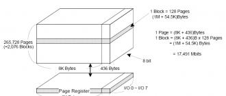
For an example of working with ROM, consider the organization of memory and access to it using the example of a NAND memory chip.
The structure of NAND memory is shown in Figure 8.2.

The memory in the microcircuit is divided into blocks, which in turn are divided into pages, consisting of bytes. That. to fully address a byte of memory, you need to know the block number, the page number and the byte address itself in this page.
The total memory capacity in this case is equal to the product of the page capacity by the number of pages in a block and by the number of blocks in the memory chip. If we have, as shown in Figure 8.2, the microcircuit consists of 2000 blocks containing 128 pages each. The page contains 8192 bytes of memory. As a result, we get: 8192 * 128 * 2000 = 2 GB of memory. Usually the memory size is indicated in bits. Those. the size of the microcircuit in question is 16Gbit, which will be indicated in its documentation.
Accordingly, to obtain one byte of information at the R / W pin, which is responsible for reading and writing, a signal is set indicating that there will be reading. A command is sent to request a read byte of data. Then a package of the form is formed, as shown in Figure 8.3.

In this packet, A13-A0 is the byte address in the page, A20-A14 is the page number, A32-A21 is the block number.
In response to this request, the microcircuit must issue the requested byte. At the same time, if you need to read several bytes in a row, then it is enough just to continue reading the data without updating the address. The microcircuit automatically increments the address by one each time it is read. Those. when using this microcircuit, it is advantageous to read data at once in pages (in our example, 8192 bytes).
Articles to read:
ROM - Read Only Memory
Send your good work in the knowledge base is simple. Use the form below
Students, graduate students, young scientists who use the knowledge base in their studies and work will be very grateful to you.
Posted on http://www.allbest.ru/
Posted on http://www.allbest.ru/
Novgorod State University I. Wise
abstract
On the topic “Permanent storage devices. Main characteristics, scope "
Completed: 1st year student gr. 5261
Bronina Ksenia
Checked by: Gelirya Askhatovna Arkhipova
Veliky Novgorod, 2016
1. The concept of permanent storage
1.1 Main characteristics of ROM
1.2 Classification of ROM
1.2.1 By type of execution
1.2.2 By types of ROM chips
1.2.3 By the method of programming microcircuits (writing firmware to them)
2. Application
3. Historical types of ROM
Literature
1. The concept of permanent storage
Read only memory (ROM, or ROM - Read Only Memory, read-only memory) is also built on the basis of modules (cassettes) installed on the motherboard and is used to store unchangeable information: operating system boot programs, computer device testing programs and some drivers basic input / output system (BIOS), etc.
Permanent memory includes read-only memory, ROM (in English literature - Read Only Memory, ROM, which literally translates as "read-only memory"), programmable ROM, EPROM (in English literature - Programmable Read Only Memory, PROM), and flash memory. The name of the ROM speaks for itself. The information in the ROM is recorded at the factory-manufacturer of the memory microcircuits, and its value cannot be changed in the future. The ROM stores information that is critical for the computer, which does not depend on the choice of the operating system. The programmable ROM differs from the usual one in that the information on this microcircuit can be erased by special methods (for example, ultraviolet rays), after which the user can re-write information on it. This information cannot be deleted until the next erasing operation.
It is customary to refer to ROM as non-volatile permanent and "semi-permanent" storage devices, from which you can only read information on-the-fly, recording information in ROM is performed outside the PC in laboratory conditions or in the presence of a special programmer and in the computer. According to the information recording technology, ROMs of the following types can be distinguished:
§ microcircuits programmable only during manufacture - classic or masked ROMs or ROMs;
§ microcircuits programmable once in the laboratory - programmable ROM (PROM), or programmable ROM (PROM);
§ microcircuits programmable repeatedly - reprogrammable ROM or erasable PROM (EPROM). Among them should be noted electrically reprogrammable EEPROM (Electrical Erasable PROM) chips, including flash memory.
1.1 Main characteristics of ROM
Data in read-only memory (ROM) is stored permanently. Data stored permanently is referred to as non-volatile, which means that it is retained in ROM even when the power is turned off. Once data is written to ROM, it can be read by other devices, but new data cannot be written to ROM.
ROM is most commonly used to store what is called a “monitor program”. A monitor program is a machine program that allows the user of a microcomputer system to view and modify all system functions, including memory. Another widespread use of ROM is storing fixed tables of data, such as mathematical functions, that never change.
Four types of ROM are widely used by digital computer systems: mask-programmed ROM, programmable ROM (EPROM), erasable programmable ROM (EPROM), and electrically programmable ROM (EEPROM).
1.2 Classification of ROM
1.2.1 By type of execution
The data array is combined with the sampling device(a reader), in this case the data array is often called "firmware" in conversation:
§ ROM chip;
§ One of the internal resources of a single-chip microcomputer (microcontroller), usually FlashROM.
The dataset exists on its own:
§ compact disc;
§ punch card;
§ punched tape;
§ bar codes;
§ mounting "1" and mounting "0".
1.2.2 By types of ROM chips
By crystal manufacturing technology:
§ RO M eng. read-only memory - read-only memory, masked ROM, manufactured by the factory method. In the future, there is no way to change the recorded data.
Figure 1. Mask ROM
§ PRO M eng. programmable read-only memory - programmable ROM that can be flashed once by the user.
Figure 2. Programmable ROM
§ EPROM eng. erasable programmable read-only memory - reprogrammable / reprogrammable ROM (EPROM / EPROM)). For example, the contents of the K573RF1 microcircuit were erased using an ultraviolet lamp. For the passage of ultraviolet rays to the crystal, a window with quartz glass was provided in the microcircuit case.
Figure 3. Flash ROM
§ EEPROM eng. electrically erasable programmable read-only memory). Memory of this type can be erased and filled with data several tens of thousands of times. Used in solid state drives. One of the varieties of EEPROM is flash memory.
Figure 4. Erasable ROM
§ ROM on magnetic domains, for example K1602RTs5, had a complex sampling device and stored a rather large amount of data in the form of magnetized regions of the crystal, while not having moving parts (see. Computer memory). An unlimited number of rewriting cycles was provided.
§ NVRAM, non-volatile memory - "non-volatile" memory, strictly speaking, is not a ROM. This is a small RAM, structurally combined with a battery. In the USSR, such devices were often called "Dallas" after the company that launched them on the market. In NVRAM of modern computers, the battery is no longer structurally connected to the RAM and can be replaced.
By type of access:
§ With parallel access (parallel mode or random access): such a ROM can be accessed in the system in the address space of the RAM. For example, K573RF5;
§ With sequential access: such ROMs are often used for one-time loading of constants or firmware into a processor or FPGA, used to store TV channel settings, etc. For example, 93C46, AT17LV512A.
1.2.3 By the method of programming microcircuits (writing firmware to them)
§ Non-programmable ROM;
§ ROMs programmed only with the help of a special device - ROM programmer (both once and repeatedly flashed). The use of a programmer is necessary, in particular, to supply non-standard and relatively high voltages (up to +/- 27 V) to special outputs.
§ In-circuit (re) programmable ROM (ISP, in-system programming) - such microcircuits have a generator of all the necessary high voltages inside, and can be flashed without a programmer and even without soldering from the printed circuit board, by software.
memory chip programming monoscope
2. Application
The read-only memory is often recorded with the firmware for controlling a technical device: a TV, a cell phone, various controllers, or a computer (BIOS or OpenBoot on SPARC machines).
BootROM is a firmware, such that if it is written into a suitable ROM chip installed in a network card, it becomes possible to load the operating system onto a computer from a remote local network node. For embedded network cards, BootROM can be activated via BIOS.
ROM in IBM PC-compatible computers is located in the address space from F600: 0000 to FD00: 0FFF
3. Historical types of ROM
Permanent storage devices began to find application in technology long before the advent of computers and electronic devices. In particular, one of the first types of ROM was the cam roller, which was used in barrel organs, music boxes, and striking clocks.
With the development of electronic technology and computers, the need arose for high-speed ROMs. In the era of vacuum electronics, ROMs based on potentioscopes, monoscopes, and beam lamps were used. In computers based on transistors, plug-in matrices were widely used as ROMs of small capacity. If it was necessary to store large amounts of data (for computers of the first generations - several tens of kilobytes), ROMs based on ferrite rings were used (they should not be confused with similar types of RAM). It is from these types of ROM that the term "firmware" originates - the logical state of the cell was set by the direction of winding the wire that enclosed the ring. Since a thin wire had to be pulled through a chain of ferrite rings, metal needles similar to sewing ones were used to perform this operation. And the very operation of filling the ROM with information resembled the sewing process.
Literature
Ugryumov E.P. Digital circuitry BHV-Petersburg (2005) Chapter 5.
Posted on Allbest.ru
Similar documents
Hierarchy of computer storage devices. Microcircuits and memory systems. Random access memory devices. The principle of the memory device. Maximum permissible operating modes. Increase in memory size, bit depth and number of stored words.
term paper, added 12/14/2012
Storage devices: hard drives, floppy disks, streamers, flash memory cards, MO-drives, optical: CD-R, CD-RW, DVD-R, DVD-RW, and the latest storage devices. The information must be stored on media that does not depend on the presence of voltage.
abstract, added 03/01/2006
The concept of information, its measurement, quantity and quality of information. Storage devices: classification, principle of operation, main characteristics. Organization and facilities of the human-machine interface, multimedia and hypermedia. Spreadsheets.
practice report, added 09/09/2014
Designing a programmer for AT17C010 microcircuits, substantiating the modes of functioning of microcontroller nodes, hardware, sufficiency of software resources. Schematic diagram of the device, recommendations for the development of diagnostic tools.
term paper, added 12/19/2010
Designing elements of ROM and RAM microcircuits using the MS Visio 2010 application. Division and expansion of the address space. Calculation of additional random access memory and verification of system components for electrical interaction.
term paper added on 11/08/2014
Computer storage devices. Creation of a memory system. Characteristics of dynamic memory microcircuits. Performing arithmetic, logical or service operations. Layered-parallel form of the algorithm. The degree and levels of parallelism.
presentation added 03/28/2015
Microprocessor set of the KR580 series - a set of microcircuits. The main elements of the KR580VM80A are an 8-bit microprocessor, a full analogue of the Intel i8080 microprocessor. The use of microprocessors in slot machines. Versions of the release of microcircuits, and their application.
abstract, added 02/18/2010
Comparison of the two most important characteristics - memory capacity and its performance. General purpose registers. Functions of random access memory. The most common form of external storage is the hard drive. Three main types of optical media.
abstract added on 01/15/2015
The main components of the system unit. The purpose of the motherboard. The basic input-output system is Bios. The concept of a peripheral device. Storage devices and their types. Open architecture in a PC device. Devices for input and output of data.
abstract, added 12/18/2009
Calculation of the static module of random access memory and storage. Construction of a schematic diagram and a timing diagram of a random access memory module. Designing an arithmetic logic unit for dividing numbers with a fixed point.
ROM is a memory, information in which, once written, cannot be changed. For example, a program for loading information from external memory into the RAM of a microprocessor system. All types of ROMs use the same circuit design principle. Information in ROM is represented as the presence or absence of a connection between the address and data buses.
The conventional graphic designation of the ROM is shown in Fig. 26.10.
Fig. 26.10. Conditional graphic designation of ROM
Rice. 26.11. ROM circuit
In fig. 26.11 shows a diagram of the simplest ROM. To implement ROM, it is enough to use a decoder, diodes, a set of resistors and bus drivers. The considered ROM contains bit words, i.e. its total size is 32 bits. The number of columns determines the word length, and the number of rows determines the number of 8-bit words. Diodes are installed in those places where bits with a logical value of "0" should be stored (the decoder feeds 0 to the selected line). Currently, instead of diodes, MOS transistors are installed.
Table 26.1 shows the state of the ROM, the diagram of which is shown in Fig. 26.11.
Table 26.1
Simple ROM state
| Word | Binary representation | ||||||||
| A0 | A1 | D1 | D2 | D3 | D4 | D5 | D6 | D7 | D8 |
As a rule, ROMs have a multi-bit organization with a structure of 2 DM... Manufacturing technologies are very diverse - CMOS, n-MOS, TTL (W) and diode arrays.
All ROMs can be divided into the following groups: factory-programmable (masked), one-time programmable and reprogrammable.
In manufacturing programmable memories(ROM or ROM), information is recorded directly during their manufacture using a photomask, called a mask, at the final stage of the technological process. Such ROMs, called mask ROMs, are built on diodes, bipolar or MOS transistors.
The area of use of masked ROMs is the storage of standard information, for example, character generators (codes of letters of the Latin and Russian alphabet), tables of typical functions (sines, quadratic functions), standard software.
Programmable read only memory(EPROM, or PROM) - ROM with the possibility of one-time electrical programming. This kind of memory allows the user to program the memory chip once using the programmers.
EPROM microcircuits are built on memory cells with fusible links. The programming process consists in selectively burning off the fuse links using current pulses of sufficient amplitude and duration. Fusible links are included in the electrodes of diodes or transistors.
In fig. 26.12 shows the EPROM circuit with fusible jumpers. It is manufactured with all diodes and jumpers, i.e. in the matrix all are "0", and during programming those jumpers are burned, in the cells of which there should be logical "1".
Rice. 26.12. Fragment of the EPROM circuit
Reprogrammable read-only memory(EPROM and EPROM UV) - ROM with the possibility of multiple electrical programming. In the IC EPROM UV ( EPROM) old information is erased using ultraviolet rays, for which there is a transparent window in the microcircuit case; in RPZU ( EEPROM) - using electrical signals.
The memory cells of the EPROM are built on n-MOS or CMOS transistors. Various physical phenomena of charge storage at the boundary between two dielectric media or conductive and dielectric media are used to construct a ZE.
In the first version, the dielectric under the gate of the MOS transistor is made of two layers: silicon nitride and silicon dioxide. This transistor is called MNOS: metal - silicon nitride - oxide - semiconductor. Charge trapping centers appear at the boundary of the dielectric layers. Due to the tunneling effect, charge carriers can pass through the thin oxide film and accumulate at the interface between the layers. This charge, which is the carrier of information stored by the MOSFET, leads to a change in the threshold voltage of the transistor. In this case, the threshold voltage rises so much that the operating voltage at the gate of the transistor is not able to open it. The transistor, in which there is no charge, is easy to open. One of the states is defined as a logical unit, the second is zero.
In the second version, the gate of the MOS transistor is made floating, i.e. not related to other elements of the circuit. Such a gate is charged with an avalanche injection current when a high voltage is applied to the drain of the transistor. As a result, the charge on the floating gate affects the drain current, which is used when reading information, as in the previous version with the MOS transistor. Such transistors are called LISMOS (MOSFET with avalanche charge injection). Since the gate of the transistor is surrounded by an insulator, the leakage current is very small and the information can be stored for a long time (tens of years).
In the EPROM with electrical erasure, a second, control gate, is placed above the floating gate of the transistor. Applying voltage to it causes the charge dissipation on the floating gate due to the tunneling effect. EPROM have significant advantages over EPROM UV, since they do not require special sources of ultraviolet light for reprogramming. Electrically erasable chargers have practically supplanted ultraviolet erasable chargers.
A fragment of the EPROM circuit using double-gate transistors of the LIZMOS type is shown in Fig. 26.13. Logic zero is written in programming mode using floating gate charge. Erasure of information, i.e. floating gate discharge, means writing a logical unit. In this case, when a signal is applied along the sample line, the polled transistors open and transmit voltage U PIT on the read line.
Modern EPROMs have a data capacity of up to 4 Mbit at a clock frequency of up to 80 MHz.
26.5. Flash-memory
Basic principles of work and the type of storage elements Flash-memories are similar to EPROMs with electrical recording and erasure of information built on floating gate transistors. As a rule, due to its peculiarities, Flash- memory is allocated in a separate class. It erases either all recorded information at the same time, or large blocks of information, rather than erasing individual words. This makes it possible to exclude control schemes for writing and erasing individual bytes, which makes it possible to significantly simplify the memory circuit and achieve a high level of integration and performance while reducing cost.
Fig. 26.13. Fragment of the EPROM circuit
Modern trends in the development of electronic devices require a constant increase in the amount of memory used. Today, the engineer has access to microcircuits as volatile memory of the type DRAM characterized by extremely low cost per bit and high levels of integration, as well as non-volatile Flash-memory, the cost of which is constantly decreasing and tends to the level DRAM.
The need for non-volatile Flash-Memory grows in proportion to the advancement of computer systems into the field of mobile applications. Reliability, low power consumption, small size and low weight are obvious advantages of media based on Flash-memory versus disk drives. Taking into account the constant decrease in the cost of storing a unit of information in Flash-memory, carriers based on it provide more and more advantages and functionalities to mobile platforms and portable equipment using such memory. Among the variety of types of memory, Flash-memory based on cells NAND is the most suitable basis for building non-volatile storage devices for large amounts of information.
Currently, there are two main structures for constructing flash memory: cell-based memory NOR(OR NOT) and NAND(AND-NOT). Structure NOR(Fig. 26.14, a) consists of parallel-connected elementary cells for storing information. Such an organization of cells provides the possibility of random access to data and byte writing of information. At the heart of the structure NAND(Fig. 26.14, b) is the principle of sequential connection of elementary cells, forming groups (in one group of 16 cells), which are combined into pages, and pages - into blocks. With this construction of the memory array, access to individual cells is impossible. Programming is carried out simultaneously only within one page, and when erasing, blocks or groups of blocks are accessed.
Fig. 26.14. Structures based on NOR(a) and NAND(b)
As a result of the differences in the organization of the structure between memory NOR and NAND are reflected in their characteristics. When working with relatively large data arrays, write / erase processes in memory NAND run significantly faster than memory NOR... Since 16 adjacent memory cells NAND connected in series with each other without any contact gaps, a high area of placement of cells on the chip is achieved, which allows you to get a large capacity at the same technological standards. At the heart of flash programming NAND is the process of electron tunneling. And since it is used for both programming and erasing, low power consumption of the memory chip is achieved. The sequential structure of the organization of cells allows for a high degree of scalability, which makes NAND-Flash a leader in the memory expansion race. Due to the fact that electron tunneling occurs through the entire area of the cell channel, the intensity of charge capture per unit area y NAND-Flash lower than other technologies Flash-memory, as a result of which it has a higher number of programming / erasing cycles. Programming and reading are performed sector by sector or page by page, in blocks of 512 bytes, to emulate the common sector size of disk drives.
More detailed features of microcircuits Flash-memory can be considered on the example of crystals of the series HY 27xx (08/16) 1 G 1M firms Hynix... In fig. 26.15 shows the internal structure and pin assignment of these devices.
The microcircuit has the following conclusions:
I / O 8-15- data input / output for x16 devices
I / O 0-7- data input / output, address input or command input for x8 and x16 devices;
Ale- turning on the address latch;
CLE- turn on the command latch;
- choice of crystal;
- read permission;
- read / busy (output with open drain);
- recording permission;
- write protection
V CC- supply voltage;
V SS- general conclusion.
Fig. 26.15. External terminal diagram (a), terminal assignment (b) and structural diagram (c) Flash-memory
Address lines are multiplexed with data I / O lines on an 8 or 16 bit I / O bus. This interface reduces the number of pins used and makes it possible to move to larger ICs without changing the PCB. Each block can be programmed and erased 100,000 times. The microcircuits have an open-drain read / busy output that can be used to identify controller activity PER (Program / Erase / Read). Since the output is made with an open drain, it is possible to connect several of these outputs from different memory chips together through a single pull-up resistor to the positive terminal of the power supply.
Fig. 26.16. Organization of a memory array NAND-structures
Memory array NAND-structure is organized in blocks, each containing 32 pages. The array is divided into two areas: main and spare (Fig. 26.16).
The main area of the array is used to store data, while the spare area is usually used to store error correction codes ( ECC), program flags and bad block identifiers ( Bad block) of the main area. In 8-bit devices, the pages in the main area are divided into two half-pages of 256 bytes each, plus 16 bytes of spare area. In 16-bit devices, pages are divided into a main area of 256 words and a spare area of 8 words.
Cell-based memory NOR has relatively long erasure and write times, but has read access to each bit. This circumstance makes it possible to use such microcircuits for recording and storing program code that does not require frequent rewriting. Such applications can be, for example, BIOS for embedded computers or software for set-top boxes.
Properties NAND-Flash determined the area of its application: memory cards and other data storage devices. Now this type of memory is used almost everywhere in mobile devices, photo and video cameras, etc. NAND-Flash underlies almost all types of memory cards: SmartMedia, MMC, SecureDigital, MemoryStick
Currently achieved information capacity Flash-Memory reaches 8GB, typical cumulative programming and erase speed is up to 33.6 ms / 64 kB at clock speeds up to 70 MHz.
Two main areas of effective use Flash-Memories are storage of rarely changed data and replacement of memory on magnetic disks. For the first direction, use Flash- memory with address access, and for the second - file memory.
26.6. RAM type FRAM
FRAM- an operative nonvolatile memory, combining high speed and low power consumption inherent in RAM, with the property of storing data in the absence of an applied voltage.
Compared to EEPROM and Flash- with memory, the time for writing data to a memory of this type and the power consumption is much less (less than 70 ns versus several milliseconds), and the resource for write cycles is much higher (at least 10 11 versus 10 5 ... 10 6 cycles for EEPROM).
FRAM should become the most popular memory in digital devices in the near future. FRAM will differ not only in performance at the level DRAM, but also the ability to save data when the power is turned off. In a word, FRAM can supplant not only the slow Flash, but also the usual type of RAM DRAM... Today ferroelectric memory finds limited use, for example, in RFID-tags. Leading companies, including Ramtron, Samsung, NEC, Toshiba actively develop FRAM... By about 2015, the market should be delivered n- gigabyte modules FRAM.
Specified properties FRAM provides a ferroelectric (perovskite) used as the dielectric of the storage capacitor of the memory cell. In this case, the ferroelectric memory stores data not only in the form of a capacitor charge (as in traditional RAM), but also in the form of electric polarization of the crystal structure of a ferroelectric. A ferroelectric crystal has two states, which can correspond to logical 0 and 1.
Term FRAM not yet settled. The first FRAM got the name - ferrodynamic RAM. However, at present, a ferroelectric is used as storage cells and now FRAM often referred to as ferroelectric RAM.
The first FRAM had 2 T/2WITH-architecture (Fig. 26.17, a), on the basis of which most modern ferroelectric memory microcircuits are performed. A cell of this type, in which each bit has an individual reference bit, allows the difference in charge to be determined with high precision. And thanks to the reading of the differential signal, the influence of the spread of the parameters of the cell capacitors is excluded. Later appeared FRAM with architecture 1 T/1WITH(Figure 26.17, b). The advantage of microcircuits with such an architecture is that the cell area is smaller than in conventional circuits and, therefore, the lower cost of the microcircuit per unit of information capacity.
Figure 26.18 shows a block diagram of a ferroelectric RAM ( FRAM) with a volume of 1 Mbit and a parallel access interface FM 20L 08 companies Ramtron... Table 26.1. the pins of the microcircuit are shown.
FM 20L 08 - non-volatile memory with organization 128K × 8, which is read and written like standard static RAM. Data safety is ensured for 10 years, while there is no need to think about data storage reliability (unlimited durability), system design is simplified and a number of disadvantages of an alternative non-volatile memory solution based on battery-backed static RAM are eliminated. Recording speed and unlimited rewriting cycles make FRAM leader in relation to other types of non-volatile memory.

Fig. 26.17. Memory cell type 2 T/2WITH(a) and 1 T/1WITH(b)

Fig. 26.18. Structural scheme FRAM FM 20L 08
Computers and any electronics are complex devices, the principles of which are not always clear to most ordinary people. What is a ROM and why is a device needed? Most people will not be able to answer this question. Let's try to correct this misunderstanding.
What is ROM?
What are they and where are they used? Read-only memory (ROM) is a non-volatile memory. Technologically, they are implemented as a microcircuit. At the same time, we learned what the abbreviation for the ROM is. Devices are intended for storing information entered by the user and installed programs. In the read-only memory, you can find documents, melodies, pictures - i.e. anything that needs to be stored for months or even years. The amount of memory, depending on the device used, can vary from several kilobytes (on the simplest devices with one silicon crystal, an example of which are microcontrollers) to terabytes. The larger the ROM size, the more objects can be stored. The volume is directly proportional to the amount of data. If you condense the answer to the question of what is a ROM, the answer should be: it is one that does not depend on constant voltage.
Hard disks as primary read-only storage devices

The question of what is a ROM has already been answered. Now we should talk about what they are. The main read-only memory is hard disks. They are in every modern computer. They are used due to their wide possibilities of information accumulation. But at the same time there are a number of ROMs that use multiplexers, boot loaders and other similar electronic mechanisms). With a detailed study, it will be necessary not only to understand the meaning of the ROM. Deciphering other terms is also necessary in order to delve into the topic.
Expansion and addition of ROM capabilities thanks to flash technologies

If the standard user is not enough, then you can use the additional expansion of the provided ROM in the field of data storage. This is done through modern technologies implemented in memory cards and USB flash drives. They are based on the principle of reusable use. In other words, the data on them can be erased and written tens and hundreds of thousands of times.
What is read-only memory

The ROM contains two parts, which are designated as ROM-A (for storing programs) and ROM-E (for issuing programs). Read-only memory type A is a diode-transformer matrix that is stitched with address wires. This section of the ROM performs the main function. The filling depends on the material from which the ROM is made (perforating and magnetic tapes, punched cards, magnetic disks, drums, ferrite tips, dielectrics and their property of accumulating electrostatic charges can be used).
Schematic structure of ROM

This electronic object is depicted as a device that in appearance resembles the connection of a certain number of one-bit cells. The ROM chip, despite its potential complexity and seemingly significant capabilities, is small in size. When a certain bit is memorized, it is sealed to the body (when zero is written) or to the power source (when one is written). To increase the capacity of memory cells in read-only memory devices, microcircuits can be connected in parallel. This is what manufacturers do to get a modern product, because the high-performance ROM chip allows them to be competitive in the market.
Memory volumes when used in various equipment

The amount of memory differs depending on the type and purpose of the ROM. So in simple household appliances like washing machines or refrigerators, installed microcontrollers can be enough (from their reserves of several tens of kilobytes), and in rare cases something more complex is installed. It makes no sense to use a large amount of ROM here, because the amount of electronics is small, and complex calculations are not required from the technology. For modern TVs, something more perfect is already required. And the pinnacle of complexity is computing equipment like computers and servers, ROMs for which, at least, can contain from several gigabytes (for those released 15 years ago) to tens and hundreds of terabytes of information.
Mask ROM

In cases where the recording is carried out using a metallization process and a mask is used, such a read-only memory is called mask. The addresses of memory cells in them are fed to 10 pins, and a specific microcircuit is selected using a special CS signal. Programming of this type of ROM is carried out at factories, as a result of which manufacturing in small and medium volumes is unprofitable and rather inconvenient. But with large-scale production, they are the cheapest among all permanent storage devices, which ensured their popularity.
Schematically, they differ from the total mass in that, in the storage matrix, the conductor connections are replaced by fusible jumpers made of polycrystalline silicon. During the production stage, all jumpers are created and the computer assumes that logical units are written everywhere. But during preparatory programming, an increased voltage is applied, with the help of which logical units are left. When low voltages are applied, the jumpers evaporate, and the computer reads that there is a logical zero. This is the principle behind programmable read-only memory devices.
Programmable read only memory
EPROMs turned out to be convenient enough in the process of technological production so that they could be used in medium and small batch production. But such devices also have their limitations - for example, you can write a program only once (due to the fact that the jumpers evaporate once and for all). Because of this impossibility to reuse the read-only memory, it must be discarded in case of erroneous writing. As a result, the cost of all the equipment produced increases. Due to the imperfection of the production cycle, this problem occupied the minds of the designers of memory devices quite strongly. The way out of this situation was the development of a ROM that can be programmed anew many times.
UV or electrical erasable ROM

And such devices were called "read-only memory with ultraviolet or electric erasure." They are created on the basis of a memory matrix, in which memory cells have a special structure. So, each cell is a MOSFET, in which the gate is made of polycrystalline silicon. Similar to the previous option, right? But the peculiarity of these ROMs is that silicon is additionally surrounded by a dielectric with wonderful insulating properties - silicon dioxide. The principle of operation here is based on the content of the induction charge, which can be stored for decades. There are erasure features here. So, for an ultraviolet ROM device, it is necessary to get into ultraviolet rays coming from the outside (an ultraviolet lamp, etc.). Obviously, from the point of view of simplicity, the operation of read-only memories with electric erasure is optimal, since to activate them, you just need to apply voltage. The principle of electrical erasing has been successfully implemented in ROMs such as flash drives, which can be seen on many.
But such a ROM circuit, with the exception of cell construction, does not differ structurally from a conventional masked read only memory. Sometimes such devices are also called reprogrammable. But with all the advantages, there are certain limits to the speed of erasing information: this action usually takes about 10-30 minutes.
Despite the possibility of overwriting, reprogrammable devices have restrictions on their use. For example, UV-erasable electronics can survive 10 to 100 rewriting cycles. Then the destructive influence of radiation becomes so noticeable that they cease to function. You can see the use of such elements as storage for BIOS programs, in video and sound cards, for additional ports. But the principle of electrical erasure is optimal for rewriting. So, the number of rewrites in ordinary devices ranges from 100,000 to 500,000! There are separate ROMs that can work more, but most users don't need them.