Modern microprocessors are the fastest and smartest microcircuits in the world. They can perform up to 4 billion operations per second and are produced using many different technologies. Since the beginning of the 90s of the 20th century, when processors went into mass use, they have gone through several stages of development. The apogee of the development of microprocessor structures using the existing technologies of the 6th generation microprocessor was 2002, when it became available to use all the basic properties of silicon to obtain high frequencies with the least losses in production and creation of logic circuits. Now, the efficiency of new processors is declining somewhat despite the constant increase in the frequency of the crystals, as silicon technologies are approaching the limit of their capabilities.
Microprocessoris an integrated circuit formed on a small silicon crystal. Silicon is used in microcircuits due to the fact that it has semiconductor properties: its electrical conductivity is greater than that of dielectrics, but less than that of metals. Silicon can be made both an insulator that prevents the movement of electric charges, and a conductor - then electric charges will freely pass through it. The conductivity of a semiconductor can be controlled by introducing impurities.
The microprocessor contains millions of transistors connected to each other by the thinnest conductors made of aluminum or copper and used for data processing. This is how the inner tires are formed. As a result, the microprocessor performs many functions - from mathematical and logical operations to controlling the operation of other microcircuits and the entire computer.
One of the main parameters of the microprocessor is the frequency of the crystal, which determines the number of operations per unit of time, the frequency of the system bus, the amount of internal cache memory SRAM . The processor is marked by the frequency of the crystal. The frequency of the crystal is determined by the frequency of switching transistors from closed to open. The ability of a transistor to switch faster is determined by the manufacturing technology of the silicon wafers from which the chips are made. The dimension of the technological process determines the dimensions of the transistor (its thickness and gate length). For example, using the 90nm process that was introduced in early 2004, the transistor size is 90nm and the gate length is 50nm.
All modern processors use field-effect transistors. The transition to a new process technology allows you to create transistors with a higher switching frequency, lower leakage currents, and smaller sizes. Reducing the size allows you to simultaneously reduce the area of the chip, and hence the heat dissipation, and a thinner gate allows you to apply less voltage for switching, which also reduces power consumption and heat dissipation.
The technological norm of 90 nm turned out to be a rather serious technological barrier for many chip manufacturers. This is confirmed by the company TSMC , which is engaged in the production of chips for many giants of the market, such as companies AMD, nVidia, ATI, VIA . For a long time, she was unable to establish the production of chips using 0.09 micron technology, which led to a low yield of suitable crystals. This is one of the reasons why AMD for a long time postponed the release of its processors with technology SOI (Silicon-on-Insulator) ). This is due to the fact that it is on this element dimension that all sorts of previously not so noticeable negative factors such as leakage currents, a large scatter of parameters, and an exponential increase in heat release began to strongly manifest themselves.
There are two leakage currents: gate leakage current and subthreshold leakage. First is caused by the spontaneous movement of electrons between the silicon substrate of the channel and the polysilicon gate. Second - spontaneous movement of electrons from the source of the transistor to the drain. Both of these effects lead to the fact that it is necessary to raise the supply voltage to control the currents in the transistor, which negatively affects heat dissipation. So, by reducing the size of the transistor, first of all, its gate and the silicon dioxide layer are reduced ( SiO2 ), which is a natural barrier between gate and channel.
On the one hand, this improves the speed performance of the transistor (switching time), but on the other hand, it increases the leakage. That is, it turns out a kind of closed cycle. So the transition to 90 nm is another decrease in the thickness of the dioxide layer, and at the same time an increase in leaks. The fight against leakage is, again, an increase in control voltages, and, accordingly, a significant increase in heat generation. All this led to a delay in the introduction of a new technical process by competitors in the microprocessor market - Intel and AMD.
One of the alternative solutions is the use of technology SOI (silicon on insulator), which the company recently introduced AMD on their 64-bit processors. However, it cost her a lot of effort and overcoming a large number of incidental difficulties. But the technology itself provides a huge number of advantages with a relatively small number of disadvantages.
The essence of the technology, in general, is quite logical - the transistor is separated from the silicon substrate by another thin layer of insulator. Pluses - weight. No uncontrolled movement of electrons under the transistor channel, affecting its electrical characteristics - again. After applying the unlocking current to the gate, the channel ionization time to the operating state, until the operating current flows through it, is reduced, that is, the second key parameter of the transistor performance improves, its turn-on / turn-off time is two. Or, at the same speed, you can simply lower the unlocking current - three. Or find some compromise between increasing the speed of work and reducing the voltage. While maintaining the same unlocking current, the increase in transistor performance can be up to 30%, if you leave the frequency the same, with an emphasis on energy saving, then the plus can be even greater - up to 50%.
Finally, the characteristics of the channel become more predictable, and the transistor itself becomes more resistant to sporadic errors, such as those caused by cosmic particles that enter the substrate of the channel and ionize it unexpectedly. Now, getting into the substrate located under the insulator layer, they do not affect the operation of the transistor in any way. The only disadvantage of SOI is that you have to reduce the depth of the emitter/collector region, which directly and directly affects its resistance increase as the thickness decreases.
And finally third the reason that contributed to the slowdown in frequency growth is the low activity of competitors in the market. It can be said that everyone was busy with their own affairs. AMD engaged in the widespread introduction of 64-bit processors, for Intel it was a period of improvement of the new technical process, debugging for an increased yield of suitable crystals.
So, the need to switch to new technical processes is obvious, but it is given to technologists every time with great difficulty. The first microprocessors Pentium (1993) were produced according to the 0.8 micron process technology, then 0.6 micron. In 1995, the 0.35 micron process technology was used for the first time for the 6th generation processors. In 1997 it changed to 0.25 microns, and in 1999 to 0.18 microns. Modern processors are made using 0.13 and 0.09 micron technologies, the latter being introduced in 2004. As you can see, for these technical processes, Moore's law is observed, which states that every two years the frequency of crystals doubles with an increase in the number of transistors from them. The technological process is changing at the same pace. True, in the future, the “frequency race” will outstrip this law. By 2006 the company Intel plans to master the 65-nm process technology, and 2009 - 32-nm.
Here it is time to recall the structure of the transistor, namely, a thin layer of silicon dioxide, an insulator located between the gate and the channel, and performing a completely understandable function - a barrier to electrons that prevents leakage of the gate current.
Obviously, the thicker this layer, the better it performs its insulating functions, but it is an integral part of the channel, and it is no less obvious that if we are going to reduce the channel length (transistor size), then we need to reduce its thickness, and, moreover, very at a fast pace. By the way, over the past few decades, the thickness of this layer has averaged about 1/45 of the entire length of the channel. But this process has its end - as Intel said five years ago, if you continue to use SiO 2, as it has been for the past 30 years, the minimum layer thickness will be 2.3 nm, otherwise the gate current leakage will become simply unrealistic values .
Until recently, nothing has been done to reduce sub-channel leakage, but now the situation is beginning to change, since the operating current, along with the gate response time, is one of the two main parameters characterizing the speed of the transistor, and leakage in the off state directly affects it - to save the required efficiency of the transistor, it is necessary, accordingly, to raise the operating current, with all the ensuing conditions.
Manufacturing microprocessor is a complex process that includes more than 300 stages. Microprocessors are formed on the surface of thin circular silicon wafers - substrates, as a result of a certain sequence of various processing processes using chemicals, gases and ultraviolet radiation.
The substrates are typically 200 millimeters or 8 inches in diameter. However, Intel has already moved to 300 mm or 12-inch wafers. The new plates make it possible to obtain almost 4 times more crystals, and the yield is much higher. The wafers are made from silicon, which is refined, melted and grown into long cylindrical crystals. The crystals are then cut into thin plates and polished until their surfaces are mirror-smooth and free from defects. Then, sequentially repeating cyclically, thermal oxidation is performed (formation of a film SiO2 ), photolithography, impurity diffusion (phosphorus), epitaxy (layer buildup).
In the process of manufacturing microcircuits, the thinnest layers of materials are applied to blank plates in the form of carefully calculated patterns. Up to several hundred microprocessors are placed on one plate, the manufacture of which requires more than 300 operations. The entire process of manufacturing processors can be divided into several stages: growing silicon dioxide and creating conductive regions, testing, manufacturing the package and delivery.
The microprocessor manufacturing process begins with " cultivation "on the surface of a polished plate of an insulating layer of silicon dioxide. This stage is carried out in an electric furnace at a very high temperature. The thickness of the oxide layer depends on the temperature and time that the plate spends in the furnace.
Then follows photolithography - the process during which a pattern is formed on the surface of the plate. First, a temporary layer of light-sensitive material, a photoresist, is applied to the plate, onto which an image of the transparent sections of the template, or photomask, is projected using ultraviolet radiation. Masks are made during processor design and are used to generate circuit patterns in each processor layer. Under the influence of radiation, the exposed areas of the photolayer become soluble, and they are removed with a solvent (hydrofluoric acid), revealing the silicon dioxide underlying them.
Exposed silica is removed by a process called " etching "Then the remaining photo layer is removed, as a result of which a silicon dioxide pattern remains on the semiconductor wafer. As a result of a series of additional photolithography and etching operations, polycrystalline silicon, which has the properties of a conductor, is also applied to the wafer.
During the next operation, called " doping ", open areas of the silicon wafer are bombarded with ions of various chemical elements, which form negative and positive charges in silicon, changing the electrical conductivity of these areas.
Overlay new layers with the subsequent etching of the circuit, it is carried out several times, while for interlayer connections in the layers "windows" are left, which are filled with metal, forming electrical connections between the layers. In its 0.13 micron process technology, Intel used copper conductors. In the 0.18 micron manufacturing process and previous generation processes, Intel used aluminum. Both copper and aluminum are excellent conductors of electricity. When using the 0.18-micron process technology, 6 layers were used; when introducing the 90 nm process technology in 2004, 7 layers of silicon were used.
Each layer of the processor has its own pattern, together all these layers form a three-dimensional electronic circuit. The application of layers is repeated 20-25 times over several weeks.
The silicon wafers must initially be sufficiently thick to withstand the stresses that the substrates are subjected to during the layering process. Therefore, before cutting the plate into individual microprocessors, its thickness is reduced by 33% using special processes and dirt is removed from the reverse side. Then, a layer of a special material is applied to the reverse side of the "thinner" plate, which improves the subsequent fastening of the crystal to the case. In addition, this layer provides electrical contact between the rear surface of the integrated circuit and the package after assembly.
After that, the plates are tested to check the quality of all processing operations. To determine if the processors are working properly, their individual components are tested. If faults are detected, they are analyzed to understand at what stage of processing the failure occurred.
Electrical probes are then connected to each processor and power is applied. The processors are tested by the computer, which determines whether the characteristics of the manufactured processors meet the specified requirements.
After testing, the wafers are sent to an assembly plant where they are cut into small rectangles, each containing an integrated circuit. A special precision saw is used to separate the plate. Non-working crystals are rejected.
Each crystal is then placed in an individual case. The case protects the crystal from external influences and provides its electrical connection with the board on which it will be subsequently installed. Tiny balls of solder located at certain points on the crystal are soldered to the electrical terminals of the package. Now electrical signals can flow from the board to the chip and vice versa.
In future processors, the company Intel apply technology BBUL , which will allow you to create fundamentally new cases with less heat dissipation and capacity between the legs cpu.
After the die is installed in the package, the processor is tested again to determine if it is functional. Faulty processors are rejected, and serviceable ones are subjected to stress tests: exposure to various temperature and humidity conditions, as well as electrostatic discharges. After each stress test, the processor is tested to determine its functional state. The processors are then sorted based on their behavior at various clock speeds and supply voltages.
The processors that have passed the test go to the final control, the task of which is to confirm that the results of all previous tests were correct, and the parameters of the integrated circuit correspond to the established standards or even exceed them. All processors that pass the output control are labeled and packaged for delivery to customers.
The roots of our digital lifestyle certainly stem from semiconductors, which have enabled the creation of sophisticated transistor-based computing chips. They store and process data, which is the basis of modern microprocessors. Semiconductors, which today are made from sand, are a key component in almost every electronic device, from computers to laptops to cell phones. Even cars now cannot do without semiconductors and electronics, as semiconductors control the air conditioning system, fuel injection process, ignition, sunroof, mirrors and even steering (BMW Active Steering). Today, almost any device that consumes energy is built on semiconductors.
Microprocessors are without a doubt among the most complex semiconductor products, as the number of transistors will soon reach a billion, and the range of functionality is already amazing today. Dual-core Core 2 processors will soon be released on the almost finished 45nm Intel process, and they will already contain 410 million transistors (although most of them will be used for the 6MB L2 cache). The 45nm process is named after the size of a single transistor, which is now about 1,000 times smaller than the diameter of a human hair. To a certain extent, this is why electronics begins to rule everything in our lives: even when the size of the transistor was larger, it was very cheap to produce not very complex microcircuits, the budget of transistors was quite large.
In this article, we will look at the fundamentals of microprocessor manufacturing, but also touch on the history of processors, architecture, and look at different products on the market. You can find a lot of interesting information on the Internet, some of which are listed below.
- Wikipedia: Microprocessor. This article discusses different types of processors and provides links to manufacturers and additional wiki pages on processors.
- Wikipedia: Microprocessors (Category). See the microprocessor section for even more links and information.
PC Competitors: AMD and Intel
Founded in 1969, Advanced Micro Devices Inc. is headquartered in Sunnyvale, California, while the heart of Intel, which was founded just a year earlier, is a few miles away in Santa Clara. AMD today has two factories: in Austin (Texas, USA) and in Dresden (Germany). The new plant will be up and running soon. In addition, AMD has joined forces with IBM in the development of processor technology and manufacturing. Of course, all of this is just a fraction of the size of Intel, as the market leader today has almost 20 factories in nine locations. Approximately half of them are used for the production of microprocessors. So when you compare AMD and Intel, remember that you are comparing David and Goliath.
Intel has an undeniable advantage in the form of huge production capacity. Yes, the company today is a leader in the implementation of advanced technological processes. Intel is about a year ahead of AMD in this regard. As a result, Intel can use more transistors and more cache in its processors. AMD, unlike Intel, has to optimize the technical process as efficiently as possible in order to keep up with the competitor and release decent processors. Of course, the design of processors and their architecture are very different, but the technical manufacturing process is built on the same basic principles. Although, of course, there are many differences in it.
Microprocessor manufacturing
The production of microprocessors consists of two important stages. The first is in the production of the substrate, which AMD and Intel do in their factories. This includes imparting conductive properties to the substrate. The second stage is the test of substrates, assembly and packaging of the processor. The last operation is usually performed in less expensive countries. If you look at Intel processors, you will find that the packaging was made in Costa Rica, Malaysia, the Philippines, etc.
AMD and Intel are now trying to produce products for the maximum number of market segments, moreover, based on the minimum possible assortment of crystals. A perfect example is the Intel Core 2 Duo line of processors. There are three codenamed processors for different markets: Merom for mobile applications, Conroe for the desktop version, Woodcrest for the server version. All three processors are built on the same technological basis, which allows the manufacturer to make decisions at the last stages of production. Features can be enabled or disabled, and the current clock rate gives Intel an excellent chip yield rate. If the demand for mobile processors increases in the market, Intel may focus on the release of Socket 479 models. If the demand for desktop models increases, then the company will test, validate and package chips for Socket 775, while server processors are packaged for Socket 771. So even four-core processors are being created: two dual-core crystals are installed in one package, so we get four cores.
How chips are made
The production of chips consists in the imposition of thin layers with a complex "pattern" on silicon substrates. First, an insulating layer is created that acts as an electrical shutter. A photoresist material is then applied on top, and unwanted areas are removed using masks and high-intensity irradiation. When the irradiated areas are removed, areas of silicon dioxide will open underneath, which is removed by etching. After that, the photoresistive material is also removed, and we get a certain structure on the silicon surface. Then additional photolithography processes are carried out, with different materials, until the desired three-dimensional structure is obtained. Each layer can be doped with a certain substance or ions, changing the electrical properties. Windows are created in each layer in order to then bring metal connections.
As for the production of substrates, they must be cut from a single single-crystal-cylinder into thin "pancakes" in order to be easily cut into separate processor crystals later. Sophisticated testing is carried out at every step of production to assess the quality. Electrical probes are used to test each chip on the substrate. Finally, the substrate is cut into individual cores, non-working cores are immediately eliminated. Depending on the characteristics, the core becomes one or another processor and is enclosed in a package that facilitates the installation of the processor on the motherboard. All functional blocks go through intensive stress tests.
It all starts with pads
The first step in processor manufacturing is done in a clean room. By the way, it is important to note that such a technological production is an accumulation of huge capital per square meter. The construction of a modern plant with all the equipment easily "flies away" 2-3 billion dollars, and it takes several months to test runs of new technologies. Only then can the plant mass-produce processors.
In general, the chip manufacturing process consists of several substrate processing steps. This includes the creation of the substrates themselves, which will eventually be cut into individual crystals.

It all starts with growing a single crystal, for which the seed crystal is embedded in a bath of molten silicon, which is located just above the melting point of polycrystalline silicon. It is important that the crystals grow slowly (about a day) to ensure that the atoms are arranged correctly. Polycrystalline or amorphous silicon is made up of many assorted crystals that will result in unwanted surface structures with poor electrical properties. Once the silicon is melted, it can be doped with other substances that change its electrical properties. The whole process takes place in a sealed room with a special air composition so that the silicon does not oxidize.
The single crystal is cut into "pancakes" using a circular diamond saw, which is very accurate and does not create large irregularities on the surface of the substrates. Of course, in this case, the surface of the substrates is still not perfectly flat, so additional operations are needed.
First, using rotating steel plates and an abrasive material (such as aluminum oxide), a thick layer is removed from the substrates (a process called lapping). As a result, irregularities ranging in size from 0.05 mm to approximately 0.002 mm (2,000 nm) are eliminated. The edges of each substrate should then be rounded off, as sharp edges can cause the layers to peel off. Next, the etching process is used, when using various chemicals (hydrofluoric acid, acetic acid, nitric acid) the surface is smoothed by another 50 microns. There is no physical deterioration of the surface as the whole process is completely chemical. It allows you to remove the remaining errors in the crystal structure, as a result of which the surface will be close to ideal.
The last step is polishing, which smoothes the surface down to roughness, maximum 3 nm. Polishing is done with a mixture of sodium hydroxide and granular silica.
Today, microprocessor wafers are 200 or 300 mm in diameter, allowing chip makers to get many processors from each wafer. The next step will be 450 mm substrates, but before 2013 they should not be expected. In general, the larger the substrate diameter, the more chips of the same size can be produced. A 300mm wafer, for example, yields more than twice as many processors as a 200mm wafer.

We have already mentioned doping, which is carried out during the growth of a single crystal. But doping is carried out both with the finished substrate and during photolithography processes later. This allows you to change the electrical properties of certain areas and layers, and not the entire structure of the crystal.
The addition of a dopant may occur via diffusion. Dopant atoms fill the free space inside the crystal lattice, between silicon structures. In some cases, the existing structure can also be doped. Diffusion is carried out with the help of gases (nitrogen and argon) or with the help of solids or other sources of dopant.
Another approach to doping is ion implantation, which is very useful in changing the properties of a substrate that has been doped, since ion implantation is carried out at ordinary temperature. Therefore, existing impurities do not diffuse. A mask can be applied to the substrate, which allows you to process only certain areas. Of course, one can talk about ion implantation for a long time and discuss the penetration depth, additive activation at high temperature, channel effects, penetration into oxide levels, etc., but this is beyond the scope of our article. The procedure can be repeated several times during production.
To create sections of an integrated circuit, the process of photolithography is used. Since in this case it is not necessary to irradiate the entire surface of the substrate, it is important to use the so-called masks, which transmit high-intensity radiation only to certain areas. Masks can be compared to a black and white negative. Integrated circuits have many layers (20 or more), and each of them requires its own mask.
A thin chrome film structure is applied to the surface of a quartz glass plate to create a template. At the same time, expensive tools using an electron beam or a laser write the necessary data of an integrated circuit, as a result of which we get a pattern of chromium on the surface of a quartz substrate. It is important to understand that each modification of the integrated circuit leads to the need to produce new masks, so the whole process of making changes is very costly. For very complex schemes, masks are created for a very long time.


Using photolithography, a structure is formed on a silicon substrate. The process is repeated several times until many layers (more than 20) are created. Layers can consist of different materials, moreover, you also need to think through the connections with microscopic wires. All layers can be alloyed.
Before the photolithography process begins, the substrate is cleaned and heated to remove sticky particles and water. The substrate is then coated with silicon dioxide using a special device. Next, a bonding agent is applied to the substrate, which ensures that the photoresist material that will be applied in the next step remains on the substrate. The photoresist material is applied to the middle of the substrate, which then begins to rotate at high speed so that the layer is evenly distributed over the entire surface of the substrate. The substrate is then heated again.
The cover is then irradiated through the mask with a quantum laser, hard ultraviolet radiation, X-rays, electron beams or ion beams - all of these sources of light or energy can be used. Electron beams are mainly used for masks, X-rays and ion beams for research purposes, and industrial production today is dominated by hard UV radiation and gas lasers.

Hard UV radiation at a wavelength of 13.5 nm irradiates the photoresist material as it passes through the mask.
Projection time and focus are very important to obtain the desired result. Poor focusing will result in extra particles of photoresist material remaining, as some holes in the mask will not be irradiated properly. The same will happen if the projection time is too short. Then the photoresist structure will be too wide, the areas under the holes will be underexposed. On the other hand, excessive projection time creates too large areas under the holes and too narrow a photoresist structure. As a rule, it is very time-consuming and difficult to adjust and optimize the process. Unsuccessful adjustment will lead to serious deviations in the connecting conductors.
A special stepping projection unit moves the substrate to the desired position. Then a line or one section can be projected, most often corresponding to one processor chip. Additional micro settings may make additional changes. They can debug existing technology and optimize the process. Micro-installations usually work on areas less than 1 sq. mm, while conventional installations cover larger areas.

The substrate then proceeds to a new stage where the weakened photoresist material is removed, allowing access to the silicon dioxide. There are wet and dry etch processes that treat areas of silicon dioxide. Wet processes use chemical compounds, while dry processes use gas. A separate process is to remove the remnants of the photoresist material. Manufacturers often combine wet and dry removal so that the photoresist material is completely removed. This is important because the photoresist material is organic and, if left unremoved, can cause defects in the substrate. After etching and cleaning, you can proceed to the inspection of the substrate, which usually happens at each important stage, or transfer the substrate to a new cycle of photolithography.
Substrate test, assembly, packaging

Finished substrates are tested on the so-called probe control units. They work with the entire substrate. Probe contacts are superimposed on the contacts of each crystal, allowing electrical tests to be carried out. The software tests all the functions of each core.

By cutting from the substrate, individual nuclei can be obtained. At the moment, the probe control installations have already identified which crystals contain errors, so after cutting they can be separated from the good ones. Previously, damaged crystals were physically marked, now this is not necessary, all information is stored in a single database.
Crystal mount
The functional core then needs to be bonded to the processor package using adhesive material.

Then you need to make wire connections connecting the contacts or legs of the package and the crystal itself. Gold, aluminum or copper connections can be used.

Most modern processors use plastic packaging with a heat spreader.
Typically, the core is encased in ceramic or plastic packaging to prevent damage. Modern processors are equipped with a so-called heat spreader, which provides additional protection for the crystal, as well as a large contact surface with the cooler.
Processor testing
The last stage involves testing the processor, which occurs at elevated temperatures, in accordance with the specifications of the processor. The processor is automatically installed in the test socket, after which all the necessary functions are analyzed.
CPU it is the heart of any modern computer. Any microprocessor is essentially a large integrated circuit on which transistors are located. By passing an electric current, transistors allow you to create binary logic (on - off) calculations. Modern processors are based on 45 nm technology. 45nm (nanometer) is the size of a single transistor on a processor wafer. Until recently, 90 nm technology was mainly used.
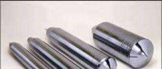
The plates are made of silicon, which is the 2nd largest deposit in the earth's crust.
Silicon is obtained by chemical treatment, purifying it from impurities. After that, it begins to be smelted, forming a silicon cylinder with a diameter of 300 millimeters. This cylinder is further cut into plates with a diamond wire. The thickness of each plate is about 1 mm. In order for the plate to have an ideal surface, after cutting with a thread, it is polished with a special grinder.
After that, the surface of the silicon wafer is perfectly smooth. By the way, many manufacturing companies have already announced the possibility of working with 450 mm plates. The larger the surface - the greater the number of transistors to accommodate, and the higher the performance of the processor.
CPU consists of a silicon wafer, on the surface of which there are up to nine levels of transistors, separated by layers of oxide, for isolation.
Development of processor manufacturing technology
Gordon Moore, one of the founders of Intel, one of the leaders in the production of processors in the world, in 1965, based on his observations, discovered the law according to which new models of processors and microcircuits appeared at regular intervals. The growth in the number of transistors in processors is growing by about 2 times in 2 years. For 40 years now, Gordon Moore's law has been working without distortion. The development of future technologies is not far off - there are already working prototypes based on 32nm and 22nm processor manufacturing technologies. Until the middle of 2004, the processor power depended primarily on the processor frequency, but starting from 2005, the processor frequency practically stopped growing. There is a new multi-core processor technology. That is, several processor cores are created with an equal clock frequency, and during operation, the power of the cores is summed up. This increases the overall power of the processor.
Below you can watch a video about the production of processors.
How microchips are made
To understand what the main difference between these two technologies is, it is necessary to make a brief digression into the technology itself for the production of modern processors or integrated circuits.
As is known from the school physics course, in modern electronics the main components of integrated circuits are p-type and n-type semiconductors (depending on the type of conductivity). A semiconductor is a substance that is superior in conductivity to dielectrics, but inferior to metals. Both types of semiconductors can be based on silicon (Si), which in its pure form (the so-called intrinsic semiconductor) is a poor conductor of electric current, but the addition (incorporation) of a certain impurity into silicon makes it possible to radically change its conductive properties. There are two types of impurities: donor and acceptor. The donor impurity leads to the formation of n-type semiconductors with an electronic type of conductivity, while the acceptor impurity leads to the formation of p-type semiconductors with a hole type of conductivity. Contacts of p- and n-semiconductors make it possible to form transistors, the main structural elements of modern microcircuits. Such transistors, called CMOS transistors, can be in two basic states: open, when they conduct electricity, and locked while they do not conduct electricity. Since CMOS transistors are the main elements of modern microcircuits, let's talk about them in more detail.
How a CMOS transistor works
The simplest n-type CMOS transistor has three electrodes: source, gate and drain. The transistor itself is made in a p-type semiconductor with hole conductivity, and n-type semiconductors with electronic conductivity are formed in the drain and source regions. Naturally, due to the diffusion of holes from the p-region to the n-region and the reverse diffusion of electrons from the n-region to the p-region, depleted layers (layers in which there are no main charge carriers) are formed at the transition boundaries of the p- and n-regions. In the normal state, that is, when no voltage is applied to the gate, the transistor is in a "locked" state, that is, it is not able to conduct current from the source to the drain. The situation does not change even if a voltage is applied between the drain and the source (we do not take into account the leakage currents caused by the movement of minor charge carriers under the influence of the generated electric fields, that is, holes for the n-region and electrons for the p-region).
However, if a positive potential is applied to the gate (Fig. 1), then the situation will change radically. Under the influence of the electric field of the gate, holes are pushed deep into the p-semiconductor, and electrons, on the contrary, are drawn into the region under the gate, forming an electron-rich channel between the source and drain. If a positive voltage is applied to the gate, these electrons begin to move from the source to the drain. In this case, the transistor conducts current they say that the transistor "opens". If the voltage is removed from the gate, the electrons cease to be drawn into the region between the source and drain, the conductive channel is destroyed and the transistor ceases to pass current, that is, it “locks”. Thus, by changing the gate voltage, you can open or close the transistor, in the same way as you can turn on or off a conventional toggle switch, controlling the flow of current through the circuit. This is why transistors are sometimes called electronic switches. However, unlike conventional mechanical switches, CMOS transistors have virtually no inertia and are capable of switching from on to off state trillions of times per second! It is this characteristic, that is, the ability to instantly switch, that ultimately determines the speed of the processor, which consists of tens of millions of such simple transistors.
So, a modern integrated circuit consists of tens of millions of the simplest CMOS transistors. Let us dwell in more detail on the manufacturing process of microcircuits, the first stage of which is the preparation of silicon substrates.
Step 1. Growing blanks
The creation of such substrates begins with the growth of a cylindrical silicon single crystal. Subsequently, round plates (wafers) are cut from such single-crystal blanks (blanks), the thickness of which is approximately 1/40 inch, and the diameter is 200 mm (8 inches) or 300 mm (12 inches). This is the silicon substrates used for the production of microcircuits.
When forming wafers from silicon single crystals, the circumstance is taken into account that for ideal crystal structures, the physical properties largely depend on the chosen direction (the anisotropy property). For example, the resistance of a silicon substrate will be different in the longitudinal and transverse directions. Similarly, depending on the orientation of the crystal lattice, the silicon crystal will react differently to any external influences associated with its further processing (for example, etching, sputtering, etc.). Therefore, the plate must be cut from a single crystal in such a way that the orientation of the crystal lattice relative to the surface is strictly maintained in a certain direction.
As already noted, the diameter of a silicon single crystal blank is either 200 or 300 mm. Moreover, a diameter of 300 mm is a relatively new technology, which we will discuss below. It is clear that a plate of such a diameter can accommodate far more than one chip, even if we are talking about an Intel Pentium 4 processor. Indeed, several dozen microcircuits (processors) are formed on one such substrate plate, but for simplicity we will consider only the processes a small area of one future microprocessor.
Step 2. Application of a protective film of dielectric (SiO2)
After the formation of the silicon substrate, the stage of creating the most complex semiconductor structure begins.
To do this, it is necessary to introduce the so-called donor and acceptor impurities into silicon. However, the question arises how to carry out the introduction of impurities according to a precisely given pattern-pattern? To make this possible, those areas where impurities are not required are protected with a special silicon dioxide film, leaving only those areas that are exposed to further processing (Fig. 2). The process of forming such a protective film of the desired pattern consists of several stages.
At the first stage, the entire silicon wafer is completely covered with a thin film of silicon dioxide (SiO2), which is a very good insulator and acts as a protective film during further processing of the silicon crystal. The wafers are placed in a chamber where, at high temperature (from 900 to 1100 °C) and pressure, oxygen diffuses into the surface layers of the wafer, leading to silicon oxidation and the formation of a surface film of silicon dioxide. In order for the silicon dioxide film to have a precisely specified thickness and not contain defects, it is necessary to strictly maintain a constant temperature at all points of the plate during the oxidation process. If not the entire wafer is to be covered with a silicon dioxide film, then a Si3N4 mask is preliminarily applied to the silicon substrate to prevent unwanted oxidation.
Step 3 Apply Photoresist
After the silicon substrate is covered with a protective film of silicon dioxide, it is necessary to remove this film from those places that will be subjected to further processing. The removal of the film is carried out by etching, and to protect the remaining areas from etching, a layer of the so-called photoresist is applied to the surface of the plate. The term "photoresist" refers to light-sensitive and resistant to aggressive factors compositions. The compositions used must, on the one hand, have certain photographic properties (become soluble under the influence of ultraviolet light and be washed out during the etching process), and on the other hand, resistive, allowing them to withstand etching in acids and alkalis, heating, etc. The main purpose of photoresists is to create a protective relief of the desired configuration.
The process of applying a photoresist and its further irradiation with ultraviolet according to a given pattern is called photolithography and includes the following main operations: formation of a photoresist layer (substrate processing, deposition, drying), formation of a protective relief (exposure, development, drying) and image transfer to the substrate (etching, deposition etc.).
Before applying the photoresist layer (Fig. 3) to the substrate, the latter is subjected to pretreatment, as a result of which its adhesion to the photoresist layer is improved. To apply a uniform layer of photoresist, the centrifugation method is used. The substrate is placed on a rotating disk (centrifuge), and under the influence of centrifugal forces, the photoresist is distributed over the surface of the substrate in an almost uniform layer. (Speaking of a practically uniform layer, one takes into account the fact that under the action of centrifugal forces the thickness of the resulting film increases from the center to the edges, however, this method of applying the photoresist allows one to withstand fluctuations in the layer thickness within ± 10%.)
Step 4. Lithography
After the application and drying of the photoresist layer, the stage of formation of the necessary protective relief begins. The relief is formed as a result of the fact that under the action of ultraviolet radiation falling on certain areas of the photoresist layer, the latter changes the properties of solubility, for example, the illuminated areas cease to dissolve in the solvent, which remove areas of the layer that have not been exposed to illumination, or vice versa - the illuminated areas dissolve. According to the way the relief is formed, photoresists are divided into negative and positive. Negative photoresists under the action of ultraviolet radiation form protective areas of the relief. Positive photoresists, on the contrary, under the influence of ultraviolet radiation acquire the properties of fluidity and are washed out by the solvent. Accordingly, a protective layer is formed in those areas that are not exposed to ultraviolet radiation.
To illuminate the desired areas of the photoresist layer, a special mask template is used. Most often, optical glass plates with opaque elements obtained by a photographic or other method are used for this purpose. In fact, such a template contains a drawing of one of the layers of the future microcircuit (there may be several hundred such layers in total). Because this pattern is a reference, it must be made with great precision. In addition, taking into account the fact that a lot of photoplates will be made using one photomask, it must be durable and resistant to damage. From this it is clear that a photomask is a very expensive thing: depending on the complexity of the microcircuit, it can cost tens of thousands of dollars.
Ultraviolet radiation passing through such a pattern (Fig. 4) illuminates only the desired areas of the surface of the photoresist layer. After irradiation, the photoresist is subjected to development, as a result of which unnecessary parts of the layer are removed. This opens the corresponding part of the layer of silicon dioxide.
Despite the apparent simplicity of the photolithographic process, it is this stage of microchip production that is the most difficult. The fact is that, in accordance with Moore's prediction, the number of transistors on a single chip is growing exponentially (doubling every two years). Such an increase in the number of transistors is possible only due to a decrease in their size, but it is precisely the decrease that “rests” on the lithography process. In order to make transistors smaller, it is necessary to reduce the geometric dimensions of the lines applied to the photoresist layer. But there is a limit to everything - it is not so easy to focus a laser beam to a point. The fact is that, in accordance with the laws of wave optics, the minimum spot size into which the laser beam is focused (in fact, this is not just a spot, but a diffraction pattern) is determined, among other factors, by the wavelength of the light. The development of lithographic technology since its invention in the early 70s has been in the direction of shortening the wavelength of light. This is what made it possible to reduce the size of the integrated circuit elements. Since the mid-1980s, ultraviolet radiation produced by a laser has been used in photolithography. The idea is simple: the wavelength of ultraviolet radiation is shorter than the wavelength of visible light, therefore it is possible to get finer lines on the surface of the photoresist. Until recently, deep ultraviolet radiation (Deep Ultra Violet, DUV) with a wavelength of 248 nm was used for lithography. However, when photolithography crossed the border of 200 nm, serious problems arose, for the first time calling into question the possibility of further use of this technology. For example, at a wavelength less than 200 µm, too much light is absorbed by the photosensitive layer, so the process of transferring the circuit template to the processor becomes more complicated and slower. Problems like these are driving researchers and manufacturers to look for alternatives to traditional lithographic technology.
The new lithography technology, called EUV lithography (Extreme UltraViolet ultraviolet radiation), is based on the use of ultraviolet radiation with a wavelength of 13 nm.
The transition from DUV to EUV lithography provides more than a 10-fold reduction in wavelength and a transition to a range where it is comparable to the size of only a few tens of atoms.
The current lithographic technology makes it possible to apply a template with a minimum conductor width of 100 nm, while EUV lithography makes it possible to print lines of much smaller widths - up to 30 nm. Controlling ultrashort radiation is not as easy as it seems. Since EUV radiation is well absorbed by glass, the new technology involves the use of a series of four special convex mirrors that reduce and focus the image obtained after applying the mask (Fig. 5 , , ). Each such mirror contains 80 individual metal layers about 12 atoms thick.
Step 5 Etching
After the photoresist layer is illuminated, the etching stage begins to remove the silicon dioxide film (Fig. 8).
The pickling process is often associated with acid baths. This method of etching in acid is well known to radio amateurs who made printed circuit boards on their own. To do this, a pattern of tracks of the future board is applied to the foil textolite with varnish, which acts as a protective layer, and then the plate is lowered into a bath with nitric acid. Unnecessary sections of the foil are etched away, exposing a clean textolite. This method has a number of disadvantages, the main of which is the inability to accurately control the layer removal process, since too many factors affect the etching process: acid concentration, temperature, convection, etc. In addition, the acid interacts with the material in all directions and gradually penetrates under the edge of the photoresist mask, that is, it destroys the layers covered by the photoresist from the side. Therefore, in the production of processors, a dry etching method, also called plasma, is used. This method makes it possible to accurately control the etching process, and the destruction of the etched layer occurs strictly in the vertical direction.
Dry etching uses an ionized gas (plasma) to remove silicon dioxide from the wafer surface, which reacts with the silicon dioxide surface to form volatile by-products.
After the etching procedure, that is, when the desired areas of pure silicon are exposed, the rest of the photolayer is removed. Thus, a silicon dioxide pattern remains on the silicon substrate.
Step 6. Diffusion (ion implantation)
Recall that the previous process of forming the necessary pattern on a silicon substrate was required in order to create semiconductor structures in the right places by introducing a donor or acceptor impurity. The process of incorporation of impurities is carried out by means of diffusion (Fig. 9) uniform incorporation of impurity atoms into the crystal lattice of silicon. To obtain an n-type semiconductor, antimony, arsenic or phosphorus are usually used. To obtain a p-type semiconductor, boron, gallium or aluminum is used as an impurity.
Ion implantation is used for the dopant diffusion process. The process of implantation consists in the fact that the ions of the required impurity are “shot out” from the high-voltage accelerator and, having sufficient energy, penetrate into the surface layers of silicon.
So, at the end of the ion implantation stage, the necessary layer of the semiconductor structure has been created. However, in microprocessors there may be several such layers. An additional thin layer of silicon dioxide is grown to create the next layer in the resulting circuit diagram. After that, a layer of polycrystalline silicon and another layer of photoresist are applied. Ultraviolet radiation is passed through the second mask and highlights the corresponding pattern on the photo layer. Then the stages of photolayer dissolution, etching and ion implantation follow again.
Step 7 Sputtering and Deposition
The imposition of new layers is carried out several times, while “windows” are left for interlayer connections in the layers, which are filled with metal atoms; as a result, metal strips are created on the crystal - conductive regions. Thus, in modern processors, links are established between layers that form a complex three-dimensional scheme. The process of growing and processing all layers lasts several weeks, and the production cycle itself consists of more than 300 stages. As a result, hundreds of identical processors are formed on a silicon wafer.
To withstand the impacts that the wafers are subjected to during the layering process, silicon substrates are initially made thick enough. Therefore, before cutting the plate into individual processors, its thickness is reduced by 33% and dirt is removed from the reverse side. Then, a layer of a special material is applied to the back side of the substrate, which improves the fastening of the crystal to the case of the future processor.
Step 8. Final step
At the end of the formation cycle, all processors are thoroughly tested. Then, specific crystals that have already passed the test are cut out from the substrate plate using a special device (Fig. 10).
Each microprocessor is built into a protective housing, which also provides electrical connection of the microprocessor chip with external devices. The package type depends on the type and intended application of the microprocessor.
After being sealed into the housing, each microprocessor is retested. Faulty processors are rejected, and serviceable ones are subjected to stress tests. The processors are then sorted based on their behavior at various clock speeds and supply voltages.
Promising technologies
The technological process for the production of microcircuits (in particular, processors) has been considered by us in a very simplified way. But even such a superficial presentation makes it possible to understand the technological difficulties that one has to face when reducing the size of transistors.
However, before considering new promising technologies, let's answer the question posed at the very beginning of the article: what is the design norm of the technological process and how, in fact, does the design norm of 130 nm differ from the norm of 180 nm? 130 nm or 180 nm is a characteristic minimum distance between two adjacent elements in one layer of the microcircuit, that is, a kind of grid step to which the microcircuit elements are bound. At the same time, it is quite obvious that the smaller this characteristic size, the more transistors can be placed on the same chip area.
Intel processors currently use a 0.13 micron manufacturing process. This technology is used to manufacture the Intel Pentium 4 processor with the Northwood core, the Intel Pentium III processor with the Tualatin core, and the Intel Celeron processor. In the case of such a technological process, the useful width of the transistor channel is 60 nm, and the thickness of the gate oxide layer does not exceed 1.5 nm. All in all, the Intel Pentium 4 processor contains 55 million transistors.
Along with increasing the density of transistors in a processor chip, the 0.13-micron technology, which replaced the 0.18-micron, has other innovations. First, it uses copper connections between the individual transistors (in 0.18 micron technology, the connections were aluminum). Secondly, 0.13 micron technology provides lower power consumption. For mobile technology, for example, this means that the power consumption of microprocessors becomes less, and the battery life longer.
Well, the last innovation that was embodied in the transition to a 0.13-micron technological process is the use of silicon wafers (wafer) with a diameter of 300 mm. Recall that before that, most processors and microcircuits were manufactured on the basis of 200 mm wafers.
Increasing the wafer diameter reduces the cost of each processor and increases the yield of products of adequate quality. Indeed, the area of a wafer with a diameter of 300 mm is 2.25 times larger than the area of a wafer with a diameter of 200 mm, respectively, and the number of processors obtained from one wafer with a diameter of 300 mm is more than twice as large.
In 2003, the introduction of a new technological process with an even lower design standard, namely 90-nanometer, is expected. The new process technology that Intel will manufacture most of its products, including processors, chipsets and communications equipment, was developed at Intel's 300mm wafer pilot plant D1C in Hillsboro, Oregon.
On October 23, 2002, Intel Corporation announced the opening of a new $2 billion facility in Rio Rancho, New Mexico. The new plant, called F11X, will use state-of-the-art technology to manufacture processors on 300mm wafers using a 0.13 micron design process. In 2003, the plant will be transferred to a technological process with a design standard of 90 nm.
In addition, Intel has already announced the resumption of construction of another manufacturing facility at Fab 24 in Leixlip, Ireland, which is designed to fabricate semiconductor components on 300mm silicon wafers with a 90nm design rule. The new enterprise with a total area of more than 1 million square meters. feet with especially clean rooms with an area of 160 thousand square meters. feet is expected to be operational in the first half of 2004 and will employ more than a thousand people. The cost of the object is about 2 billion dollars.
The 90nm process uses a number of advanced technologies. These include the world's smallest mass-produced CMOS transistors with a gate length of 50 nm (Figure 11), which provides increased performance while reducing power consumption, and the thinnest gate oxide layer of any transistor ever manufactured only 1.2 nm (Figure 12), or less than 5 atomic layers, and the industry's first implementation of high performance stressed silicon technology.
Of the listed characteristics, perhaps only the concept of “stressed silicon” needs to be commented on (Fig. 13). In such silicon, the distance between atoms is greater than in a conventional semiconductor. This, in turn, allows the current to flow more freely, similar to how vehicles with wider lanes move more freely and faster.
As a result of all innovations, the performance of transistors is improved by 10-20%, while increasing production costs by only 2%.
In addition, the 90nm process uses seven layers per chip (Figure 14), one more layer than the 130nm process, and copper connections.
All of these features combined with 300mm silicon wafers provide Intel with performance, volume and cost advantages. Consumers benefit as well, as Intel's new process technology allows the industry to continue to evolve in accordance with Moore's Law, improving processor performance time and time again.