Often to quickly assemble a layout of some electronic circuit on the table, convenient to take advantage macatetiewhich allows you to do without soldering. And only then, when you see for the performance of your scheme, you can take care of the creation of a circuit board with soldering. For a person, only a beginner to know the world of electronics, it is not obvious to the use of such a tool as a breadboard or Bradboard (Breadboard). Let's see what is a batch fee and how to work with it.
Instructions for working with an invoko dumping board (Braddatrad)
We need:
- Breadboard, buy;
- connecting wires (I recommend this set);
- lED (you can buy);
- resistor resistance 330 Ohms or close to this (a great set of resistors of all popular denominations);
- croon type battery for 9 volts.
1 Descriptionmacateboards
Macateboards there are many types. They differ in the number of conclusions, the number of tires, configuration. But all of them are arranged according to one principle. The dumping board consists of a plastic base with a plurality of holes located usually with a standard pitch of 2.54 mm. With the same step, legs are usually located at the output chip. Holes are needed in order to insert the findings of radio elements or connecting wires. A typical view of the dumping board is presented in the figure.
Various types of breadboard
His British name - Breadboard ("Bread Board") - This type of boards received due to comparison with a bumping board: it is suitable for quick "preparation" of simple schemes.
There are also exist macateboards Under soldering. They differ in the fact that they are usually made of fiberglass, and their metallized platforms are well suited for soldering wires and output radio elements. In this article, we do not consider such fees.
2 Devicemacateboards
Let's see what inside the batade. The figure below shows a general view of the board. On the right side of the picture, the conductor tires are indicated. Blue colour - this is "minus" schemes, red - "plus", green - these are conductors that you can use at your discretion for parts connections electrical circuitCollected on the Male Plate. Please note that the central holes are connected by parallel rows of the pale board, and not along. Unlike the power tires, which are located along the edge of the dummy board along its edge. As can be seen, there are two pairs of power tires, which allows you to apply two on the fee different stresses, for example, 5 V and 3.3 V.
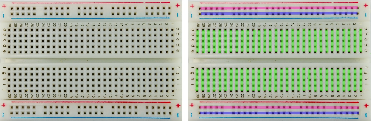 Device of the Make Plata (Breadboard)
 Two groups of transverse conductors are separated by a wide groove. Thanks to this deepening, chips in DIP-enclosures can be placed on the dump fee (housings with "legs"). As in the figure below:

There are also radio elements for surface mounting (their "legs" during installation is inserted out not in the holes in the printed circuit board, but solder directly to its surface). It is possible to use them with a similar dealer only with special adapters - clamping or under the soldering. Universal adapters are called "zero-gain panels" or Zif panel using foreign terminology. Such adapters are most often under 8-pin chips and under 16-pin chips. An example of such elements and such an adapter is shown in the illustration.

The numbers and letters on the dumping board are needed so that you can easier to navigate on the board, and if necessary, draw and sign your own concept. It can sometimes be useful when installing large schemes, especially if you mount the description. To use them in about the same way as letters and numbers on a chessboard, for example: connect the output of the resistor into the nest E-11, etc.
3 Collect the schemeon a dumping board
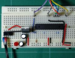
To acquire the skill of working with a batch fee the simplest scheme, as it shown on the picture. Plus batteries by connecting to the plus tire of the dummy board, "minus" - to the negative tire. Bright red and black lines are connective wires, and pale translucent are connections that provide a bold board, they are shown for clarity.
I welcome everyone. Speech today will go about the battle board. The radio amateurs will understand without any questions, since almost all at the beginning of their formation took place through the crafts. For the rest, a little more in detail. The dumping fee is needed for temporary installation of radio components when debugging electronic circuits and solving problems that occur at the device manufacturing stage.
In the times of my youth and total deficit, the dumping fees were made independently from a piece of foil Ghetinaks or a fiberglass, drawing a copper coating into the cell that there would be many sites to which radio component contacts could be soldered according to the scheme. It was justified because it was quite difficult to make a fee. It even happened that the homemakes remained in the original version on the dumping board, since no one sees inside the body, as an ax, everything is manufactured, and the scheme works and the initial goal is achieved. Saving time and resources is evident.
The homemade dummy card often looked like this: 
But time went, the progress did not stand in place. With the growth of the skills of the scheme, it became more difficult, the number of conclusions and points of the soldering increased proportionally and homemade dumping fees (layers) no longer closed the problem in full. This is where industrial dumping fees began to appear, or rather, they existed before, but were not available to everyone. And if for the guys with a radio frame at first to make the radio or the colorwoman was achievement, then later the scheme with digital logic in the implementation became even more complicated. After all, it was necessary to drill a lot of small holes and draw the conductors with a lacquer for nails, and at the end to ride in a copper cune. And if errors were made in the manufacture, then appearance Boards rapidly rolled to terrible.
This is also a batch board, but already industrial manufacture: 
In the abundance of wires, some kind of clone of the spectrum is guessed.
At the moment there are various email modern technologies manufacturing boards, including orders of small series at factories for a relatively low price. But the bold fees in any case occupy their niche and sooner or later they have to use.
Order and delivery
In general, in the dumping board (hereinafter laying) did not need much, since the manufacture of electronics does not do professionally and exclusively for himself. But seeing accidentally on sale, I decided to order. The fee was ordered in November last year, came to simple package Without puffers, about a month. There was nothing inside the fee. Damage, taking into account the fragility of the Getynaks, was not.
She looks like this: 

The color of the copper foil is pleasant, almost natural. The macateboard paths are covered with a protective composition resembling a weak solution of rosin in alcohol. At least when soldering, the amount of smoke minimally and traces of the root rosin is not observed.
The dimensions are declared 9x15 cm, in fact it is, the thickness is 1 mm, which in my opinion is not enough taking into account the properties of the material. The foil layer has a thickness of about 20 microns. 
last date calibration \u003d)

My micrometer is 31 years old, therefore, conditional testimony. In production, the minimum foil thickness of 18 microns, which corresponds to the cheapest option.
On the board of 30 rows of 48 holes that in the end gives 1440. The latter are extruded in the process of formation of the board. Drilling such a number of holes is economically inappropriate. The diameter of the holes is 1 mm. Unfortunately, the parts with the conclusions of 0.7 and 0.8 mm under the solder you have to be fixed, but it is tormented by falling.

Contact sites in the form of an octagon size 2 mm. No metallization in the holes. Since the resource of the board is minimal and the price with metallization will be unreasonably overestimated.

The basis of the grazing fee of Getinax
Getinaks - an electrically insulating layered extruded material having a paper base impregnated with phenolic or epoxy resin.
Basically used as the basis of blanks printed circuit board. Material has low mechanical strength, easily processed and has a relatively low cost. It is widely used for the cheap manufacture of boards in low-voltage household apparatus, since in a preheated state, it allows for stamping, thereby turning out the board of any form with all the holes.
Immediately recall the fees from televisions. Because of low resistance to mechanical and thermal loads, Getynaks-based fees have less maintainability and in some cases were even sources of fire ...
Trial application:
I use these ingredients
For soldering 
Solder with rosin inside, Natural rosin, soldering iron 25 W, the temperature of the sting approximately 330-350 degrees without adjustment.
And for cutting engraver FILT + set of chinese cutters 

cutters of course creepy in terms of quality, bought on new Year JD did not resist.
A reason to assemble the power supply for the signal generator + 5V + 12V-12B. At first, I wanted to drive a charging from a mobile phone by dominant windings, but I did not find any one with a normal clearance under the wires. Therefore, the choice fell on the laype.
The transformer of an unknown breed played a screw joke with me - since the pitch of the holes on the board is 2.54mm - inch, it was necessary to reap the holes at the place. The board will be thrilled easily, and even a stupid drill does not particularly slow down the drilling process, although knocks out back side Slices board.
Several photos of the finished power supply. Just the case when I decided not to make a fee.


Stabilizer 7912 played a cruel joke with me - Codovka conclusions do not correspond to 7812. Because of this, I burned the diode bridge KC407. Realizing your mistake made a turnup. When I turned off, one contact site fell off. So the quality of the board is to ride a couple of times and go to the new one.
The contact pads of Ludil almost without rosin, the one that in the solder was enough.

How many I have not tried, I could not make a droplet on the contact, it always stretches for a soldering iron. Perhaps the temperatures are not enough.
Trouble cut off


It seems that the turns are high, but Getinaks crumbs. However, the dust is not so harmful as in the fiberglass.
Why bought this particular layout and not more advanced - for rare application and to throw out it was not a pity. I do not use metallization practically. The sinking fee without soldering is also purchased, but still lies without use. Her compared to the observed disadvantage - the conclusions of the desired length and molded are required. And since I have huge stocks of old and including used parts (I swear to constantly throw everything out), then the solder is the only correct option.
Conclusions: budget layout. If not in stock, a couple can be kept.
And where is it where?
I plan to buy +13 Add to favourites I liked the review +24 +39Harbor triggered in the comments. Many supporters of Arduins, according to them, just want to simply collect the type of flashing LEDs in order to diversify their leisure and play. At the same time, they do not want to mess with etching boards and soldering. As one of the alternatives, Comrade mentioned the constructor "Expert", but its ability is limited to a set of details included in the kit, and the designer is still children. I want to offer another alternative - the so-called Breadboard, the dumping board for installation without the use of soldering.
Caution, many pictures.
What it is and with what it eats it
The main purpose of such a board is the design and debugging of prototypes various devices. Consists this device From the holes-nests with a pitch of 2.54mm (0.1 inches), it is with such (or a multiple to it) a step of conclusions on most modern radio components (SMD-non-account). Macateboards are different sizes, but in most cases they consist of these same blocks:The circuit of electrical connections of the sockets is depicted on the right figure: five holes on each side, in each of the series (in this case, 30) are electrically connected. On the left and right is two lines of food: here all holes in the column are interconnected. The slot in the middle is intended for installation and convenient extraction of chips in DIP-enclosures. To assemble the scheme in the holes, radio components and jumpers are inserted into the holes, since I got the board without factory jumpers - I did them from metal stationery clips, and small (for connecting neighboring nests) from the stapler bracket.
It may seem that the more the fee is the greater its functionality, it is not quite so. A very small chance that someone (especially from beginners) will collect a device that will take all segments of the board, here are several devices at the same time - it is yes. For example, here I assembled electronic ignition on a microcontroller, multivibrator on transistors and frequency generator for LC meter: 
So what can you do about it?
To justify the title of the article, I will give a few devices. A description of what and where to insert will be in the images.Subject details

In order to collect one of the following schemes described below, the BreadBoard type and a set of jumpers will be needed. In addition, it is desirable to have a suitable power source, in the simplest case - the battery (s), for the convenience of it (their) connections, it is recommended to use a special container. You can use the power supply, but in this case you need to be careful and try to burn anything, since the PB is much more expensive than the batteries. The remaining parts will be given in the description of the diagram itself.
Connecting LED
One of the simplest structures. On concept schemes are depicted as follows:
From the details you will need: a low-power LED, any resistor on 300Ω-1 and the power supply by 4.5-5V. In my case, the resistor is a powerful Soviet (first-hand) at 430 (as evidenced by the C43 inscription on the resistor itself), and as a power source - 3 fingers (type AA) batteries in the container: Total 1.5V * 3 \u003d 4, 5V.
On the board it looks like this:

Batteries are connected to red (+) and black (-) terminals from which jumpers are drawn to power lines. Then the resistor is connected from the minus line to the sockets No. 18, on the other side, the LED is connected to the same cathode sockets (short-leg). The anode of the LED is connected to the positive line. I will not go into the principle of operation of the scheme and explain the law of Om, I will not - if I just want to play, then it is not necessary, and if it's still interesting, then you can also.
Linear voltage stabilizer
Maybe this is a rather sharp transition - from the LED to chips, but in terms of implementation I do not see any difficulties.So, there is such a LM7805 microchip (or just 7805), it is fed to the input to any voltage from 7.5V to 25V, and we get 5V at the output. There are other, for example, a chip 7812 - 12V. This is the inclusion scheme:

Capacitors are used to stabilize the voltage and if desired, you can not install. That looks like in life:

And close-up:

The numbering of the conclusions of the chip goes left to right if you look at it from the labeling side. In the photo, the numbering of the conclusions of the microcircuit coincides with the numbering of the bradboard connectors. The red terminal (+) is connected to the 1st leg of the chip - input. The black terminal (-) is directly connected to the minus power line. The middle leg of the chip (general, GND) is also connected to the minus line, and the 3rd leg (output) to the positive line. Now, if you submit a voltage of 12V on the terminals, there should be 5V on the power lines. If there is no power source to 12V, you can take a 9B type battery and connect it through a special connector shown in the photo above. I used a 12V power supply unit:

Regardless of the input voltage value, if it lies in the above limits - the output voltage will be 5V:

Finally, add condensers to all be according to the rules:

Impulse generator on logical elements
And now an example of using another chip, if not in its most standard application. A 74HC00 or 74HCT00 chip is used, depending on the manufacturer's company before the title and after it can stand different letters. Domestic analog - K155L33. Inside this chip, 4 logical elements "and not" (eng. "Nand"), each of the elements two inputs, by closing them between them, we obtain the element "not". But in this case logic elements will be used in an "analog mode". The generator scheme is this:
Elements DA1.1 and DA1.2 generate a signal, and Da1.3 and Da1.4 - formed clear rectangles. The generator frequency is determined by the ratings of the capacitor and the resistor and is calculated by the formula: F \u003d 1 / (2RC). Connect any speaker to the generator output. If you take a resistor at 5.6k and the condenser on 33nf we get about 2,7kHz - a kind of signer sound. That looks like:

On the upper photo of the power line is connected 5V from the previously assembled voltage stabilizer. For convenience, I will give a verbal description of the compounds. Left half of the segment (Lower in the photo):
The condenser is installed in sockets No. 1 and No. 6;
Resistor - №1 and №5;
№1 and №2;
№3 and №4;
№4 and №5;
№2 and №3;
№3 and №7;
№5 and №6;
№1 and "plus" nutrition;
№4 and "plus" dynamics;
Moreover:
The microcircuit is installed as in the photo - the first leg into the first connector of the left half. The first leg of the chip can be determined by the so-called key - a mug (as in the photo) or a semicircular neckline in the end. The remaining legs of the IS in the DIP-housings are numbered counterclockwise.
If everything is assembled correctly - when the power is applied, the speaker must be written. Changing the somes of the resistor and the capacitor can be traced behind the frequency changes, but with a high resistance and / or too low capacity the scheme will not work.
Now I will change the value of the resistor at 180k, and the 1MKF capacitor is obtained by a claking-tick sound. I will replace the speaker on the LED by connecting the anode (long leg) to the 4 connector of the right rug, and the cathode through the resistor 300Ω-1k to the minus of the power supply, we get a flashing LED that looks like this:

And now add another same generator so that such a scheme is:

Generator on DA1 generates a low-frequency signal ~ 3 Hz, DA2.1 - DA2.3 - high-frequency ~ 2,7kHz, DA2.4 is a modulator that mixes them. Here is such a design:

Connection Description:
Left half of the segment (Lower in the photo):
C1 condenser is installed in sockets No. 1 and No. 6;
Capacitor C2 - №11 and №16;
Resistor R1 - №1 and №5;
Resistor R2 - №11 and №15;
Jumpers are installed between the following jacks:
№1 and №2;
№3 and №4;
№4 and №5;
№11 and №12;
№13 and №14;
№14 and №15;
№7 and minus power line.
№17 and minus power line.
Right half of the segment (top photo):
Jumpers are installed between the following jacks:
№2 and №3;
№3 and №7;
№5 and №6;
№4 and №15;
№12 and №13;
№12 (13) and №17;
№1 and "plus" nutrition;
№11 and "plus" nutrition;
№14 and "plus" dynamics;
Moreover:
jumpers between connectors №6 left and right halves;
jumpers between connectors №16 left and right halves;
- between the left and right "minus" lines;
- between the minus power and "-" dynamics;
The DA1 microcircuit is installed in the same way as in the previous case - the first leg into the first left half connector. The second chip - the first leg into the number 11 connector.
If you do everything correctly, then when the speaker is applied, the speaker will begin to produce three peak every second. If in the same connectors (in parallel), connect the LED, observing the polarity, it will turn out such a device, resembling the sounds of steep electronic pieces of no less steep militants:
Multivibrator on transistors
This scheme is more likely to tribute to tradition since in the old days almost every novice radio amateur collected similar.
In order to assemble this, 2 transistors BC547, 2 of the resistor at 1.2k, 2 resistors on 310Ω, 2 electrolytic capacitor on 22 MCF and two LEDs. Capacities and resistance are not necessarily observed accurately, but it is desirable that there are two identical nominal in the diagram.
On the board, the device is as follows:

Transistor COing Next:

B (b) -base, C (K) -ollector, E (E) -Emitter.
Capacitors have a minus exit on the housing (in Soviet capacitors signed "+").
Connection description
The whole scheme is collected on one (left) half of the segment.
Resistor R1 - №11 and "+";
Resistor R2 - №19 and "+";
Resistor R3 - №9 and №3;
Resistor R4 - №21 and №25;
Transistor T2 - Emitter -№7, base - №8, collector - №9;
transistor T1 - Emitter -№23, base - №22, collector - №21;
Condensant C1 - minus - №11, plus - №9;
Capacitor C2 - minus - №19, plus - №21;
LED LED1 - cathode-№3, anode - "+";
LED LED1 - cathode-№25, anode - "+";
Jumpers:
№8 - №19;
№11 - №22;
№7 - "-";
№23 - "-";
When the voltage is 4.5-12V, the power line should be approximately following:
Finally
First of all, the article is focused on those who want to "play", so I did not give descriptions the principles of work of schemes, physical laws, etc. If anyone led the issue "But why is it blinking?" - On the Internet you can find heaps of explanations with animations and other beautifully beautiful. Someone can say that Bradleboard is not suitable for compiling complex schemes, but what about this:
And there are even more scary structures. Regarding the possible bad contact - when using parts with normal legs, the likelihood of bad contact is very small, I have it happened only a couple of times. In general, such fees have already emerged here several times, but as part of the device built on Arduino. Honestly, I do not understand the design of the type of this:

Why do you need Arduino at all, if you can take a programmer, to flash the controller in the DIP package and install it in the fee, having received a cheaper, compact and portable device.
Yes, the Breadboard cannot collect some analog schemes sensitive to the resistance and topology of conductors, but they come across not so often, especially among beginners. But for digital circuits there are almost no restrictions.
If the first part of the article focuses on the overview of the bias and the description of their device, then now consider some useful subtleties and nonsions that you need to know when working with such dumping fees.
If the Instructions of the Inpaid Macate Fee says that the diameter of the wire inserted into contacts is 0.4 - 0.7 mm, then you should not try to insert the findings of parts that the thickness of the specified value. This will bring to weaken and wear contacts. If there is a need to apply such parts, then it is better to roll to the thick conclusions of the wire of the specified diameter, or simply wrap. Naturally, the wire must be without isolation.
Clearchy dump trucks are sold in two configurations: with wires - jumpers and without them. In the first version, the fee is obtained somewhat more expensive, but not at all troubles, if you managed to buy a single fee, - you can always adapt anything.
The switching wires, of course, are sold separately, but if there is no desire or to buy them, it is quite suitable for the KSVV 4 * 0.4 Wire, used for mounting.
Such a wire contains 4 insulated veins with a diameter of just 0.4 mm. Isolation from the wire is easily removed by rake or knife, and the residential veins do not have a varnish coating.
In case of the need to make a complex device, its individual functionally completed parts are better to collect on separate sizes of small sizes, after which it is from the obtained nodes to collect the entire design.
Sometimes it happens that one device is not yet collected, but for some reason it is necessary to urgently assemble another, completely new. And here it begins! It is necessary to disassemble the collected, not yet debt scheme, which, then, may have to be collected again. But the only irreplaceable resource is the time that is lost on these meaningless assemblies - disassembly. Therefore, it is better not to notice, but to acquire several dumping boards, it will go faster.
 We should not forget that the bold fees are designed for low-current equipment - and. Therefore, in no case in any case, it is unacceptable to supply network voltage on them - 220 V. It can lead to overheating of contacts and a breakdown of isolation, and what will happen after that everything is probably known.
But even in transistors and chips, a short circuit may occur, which will cause overheating of these elements, will lead to the heating of contacts and melting the plastic base of the board. Therefore, when you first turn on the circuit, it is desirable to measure the current consumed or at least check the temperature of all elements with a finger.
General rule, not only for dumping boards. First, components are installed not exposed to static electricity:, and.
In addition to the details, connective wires are installed on the dumping board. Connecting wires are better installed with tweezers or small pliers. With these tools to conduct and disassemble the wires.
As in all such cases Check the board on the correct installation, on the absence of short circuits or non-contacts. Unused conclusions by chips do not leave "hanging in the air", and connect either to a common wire or to the power bus. Free inputs will lead to the appearance of such elements, simply no interference, which will be distributed throughout the circuit and its adjustment will be much more problematic.
 Probably, it will have to be noted here that the dumping fees have a large fitting capacity due to long connecting wires, as well as many contacts. Therefore, too high-frequency schemes on such fees will work badly, and may not be completely.
To avoid the influence of long conductors, it is desirable to shut nutrition conclusions by microcircuit ceramic condensers Small capacity, as is done on printed circuit boards.
Checking the installation of the installation, you can use "oak" chips TTLwhich are practically not sensitive to statics. You can, of course, do without them, but it is not very convenient to overtake the cream of the multimeter into the holes on the board, it is more convenient to touch the legs of the chip. After completing the inspection and eliminating the inaccuracies, "training" chips should be replaced by real.
When using the CMOS structure chips to protect against statics, the use of antistatic grounding bracelets is very desirable. If there are no such available, you can recommend the use of a wire washcloth for washing pan. Such a mustache has the shape of a ring where you can push your hand. With the help of a flexible wire through a resistor resistance to no more than 1m connected to grounding.
After checking the circuit, you can insert the CMOS microcircuits mentioned in the fee. When setting up the scheme, replacing parts, or making changes, the protective antistatic bracelet is better not to remove.

This is a very simple use option. Of course, there are programs that help to create schemes and model devices and sometimes they benefit from inconceptuous boards. Since you yourself make any needed. But then there are small minuses. Since in practice, the parameters can differ slightly from the source data for various reasons and make sure you can only when the device is ready. Therefore, many advise first to simulate the device on the computer, then collect on the inconvenient dump truck, and then send it into production. Therefore, if you are a novice specialist or have already reached certain skills in modeling and production electronic devicesyou will be able to appreciate her to dignity and have always at hand as required tool. It will be able to turn the heavy process into a fairly light and interesting, as well as speed up the creation of your invention.