We present to our readers an overview of the power supply unit for the Canon LaserBase MF-5630 multifunctional device, which belongs to the latest generation of devices. As it already becomes a tradition, acquaintance with the circuitry of the device begins with an overview of its power supply. And, in principle, this is logical, because the operation of any electronic device begins with the start-up and normal functioning of the power supply unit.
Power supply unit Canon LaserBase MF-5630 is a single-ended pulse converter that generates five supply voltages:
- voltage + 3.5V1;
- voltage + 3.5V2;
- voltage + 5V1;
- voltage + 5V2;
- voltage + 14V;
- voltage + 24V.
In addition, on the power supply board, as befits laser devices, there is a stove control circuit, which, in turn, is controlled by signals FSRD and RLYD coming from the microprocessor to the CN1 connector of the power supply.
Signal FSRD controls the TRA1 triac through the galvanic isolation element - the PC2 optocoupler, and the signal RLYD intended for relay control RL1.
The power supply board is connected to the controller board using two interface connectors: CN101 and CN102.
The power supply is controlled by a microprocessor via a signal ON / OFF... This signal allows or, conversely, prohibits the formation of two voltages: + 3.5V2 and + 5V2. The disconnection of these voltage channels is carried out when the device goes into standby mode of operation.
The LaserBase MF-5630 power supply unit cannot be attributed to any very complex and extraordinary circuits, although it uses several solutions that deserve a separate mention.
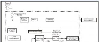
The general block diagram of the power supply, giving an idea of its main nodes and their interaction, is shown in Fig. 1. The block diagram reflects not only the main components of the power supply, but also the main electronic elements that make up this unit.
Fig. 1 Block diagram of the power supply of the Canon LaserBase MF-5630 MFP
If we correlate this block diagram with the schematic diagram shown in Fig. 2 and Fig. 3, then the purpose of all electronic components of the power supply, in principle, will become clear. However, it is still necessary to make some comments.
Fig. 2 Primary power supply for Canon LaserBase MF-5630 MFP
The primary part of the pulse converter is shown in Fig. 2. The converter is made according to an autogenerating circuit, i.e. switching moments of the power transistor Q1 are determined by EMF pulses induced in the additional winding ( pin 1-pin 2) of the transformer T1, and the ratings of the timing circuit consisting of the capacitor C10 and the resistor R6. The duration of the control pulses at the gate of Q1 can be limited by the transistor Q2, which, in turn, is controlled by the feedback signal received from the optocoupler PC1.
A very interesting feature of the primary part of the power supply is the use of an active snubber (a snubber is a damping chain). The snubber provides limitation of voltage pulses arising in the primary winding of the transformer T1 ( pin 7-pin 5) at the moment of closing the power transistor Q1. These pulses can damage Q1, so they need to be limited. The main element of the snubber is the powerful transistor Q20, which turns on when Q1 turns off. Opening, Q20 connects capacitor C20 in parallel with the primary winding, which shunts this winding, thereby limiting the EMF pulse.
Fig. 3 Secondary part of the power supply of the Canon LaserBase MF-5630 MFP
All secondary voltages are obtained by half-wave rectification of pulses induced in the secondary windings of the transformer T1. To obtain voltages with a nominal value + 5V controlled stabilizers such as PQ05RD11(IC201 and IC202). Stabilizer PQ05RD11 has the following main characteristics:- low voltage drop: no more than 0.5V;
- output current up to 1 A;
- input voltage up to 20V;
- power dissipation: 14W;
- the value of the output voltage: from 4.85V to 5.15V.
The stabilizer is controllable, i.e. it can be turned on / off by giving a corresponding signal to pin 4. Setting this pin to a high signal triggers the stabilizer, and setting the signal ON / OFF low level blocks its operation and output voltage + 5V absent.
Stabilizer IC201 is designed to generate voltage + 5V1 and it starts only after the channel voltage appears and reaches a given level + 14V. This is provided by the Zener diode D202 and the resistive divider R204 / R201. In addition, the zener diode also provides protection against short circuit and overload in the channel. + 14V... When the channel voltage + 14V decreases significantly, then the Zener diode D202 closes, which leads to the shutdown of the stabilizer IC201 and the loss of voltage + 5V1... Naturally, the corresponding circuits of the device are turned off at the same time, protecting it from operation in the event of a short circuit.
Stabilizer IC202 is designed to generate voltage + 5V2 and it starts only after the voltage appears at the output of the power supply + 3.5V2.Lack of voltage + 3.5V2 will lead to a lack of tension + 5V2 .
The voltage generation channels are also controlled. + 3.5V2 and + 24V. In these channels, keys are installed that allow or prohibit the supply of these voltages to the output of the power supply, i.e. into the load.
Key Q333, opening of which leads to the appearance of voltage at the output of the power supply + 3.5V2, controlled by a signal ON / OFF generated by the central microcontroller of the device. Setting this signal to a high level leads to the appearance of two voltages at the output of the power supply unit. + 3.5V2and + 5V2 .
The Q303 key switches the channel voltage + 24V and turns on only after the voltage appears + 5V2 .
Thus, in the considered power supply unit, alternate connection of loads of different channels is used. The sequence of appearance of the output voltages is as follows:
+ 3.5V1 / + 14V – + 5V1 - Activation ON / OFF – + 3.5V2 – + 5V2 – + 24V.
The feedback loop in this power supply is typical. It uses the PC1 optocoupler as a galvanic isolation element. The LED current of this optocoupler is regulated by a TL431 type controlled stabilizer microcircuit (only in this circuit its analogue TA76432 - IC101 is used). Channel voltage is applied to control input IC101 + 3.5V1 through the divider R115, R117, VR101, i.e. voltage + 3.5V1 is the main voltage of the power supply, on which the feedback operates.
In addition, a trigger on transistors Q112 / Q113 can control the LED current of the PC1 optocoupler. More precisely, this trigger, when triggered, creates a maximum current through the LED of the optocoupler, which leads to the setting of the feedback signal to the maximum value and, as a result, to turn off the power supply. Transistors Q112 / Q113 are a trigger for protection against overvoltage of the output voltages of the power supply. Overvoltage protection is implemented, as usual, on zener diodes:
- Zener diode D106 - protection against excess in the + 14V channel;
- Zener diode D109 - protection against excess in the + 5V1 channel;
- Zener diode D105 - protection against excess in the + 5V2 channel;
- Zener diode D107 - protection against excess in the + 24V channel.
Opening any of these zener diodes will trigger the trigger and further turn off the power supply.
Canon LBP-1120 laser printer source has classic construction for this type of printers, but there is also its own peculiarity, it is the use of a special PWM controller as a control microcircuit. It should be noted that sources based on this microcircuit are very often found in other laser printers and MFPs, for example, from HP. Structurally, the printer power supply is located on the printer control board. This board also contains the high voltage power supplies for the primary charge, development and transfer rollers, see fig. 1. The block diagram of the power supply unit is shown in Fig. 2.
The printer power supply generates stabilized voltages of + 24V used to power motors, high voltage sources, solenoids, relays, fans, etc .; as well as + 5V and + 3.3V, which is required to power the controller and formatter microcircuits, memory, optocoupler LEDs, sensors, laser, interface circuits, etc. Consider the operation of the power supply components (see Fig. 3).
The connector for the network cable of the printer is indicated on the diagram INL101. The input circuits of the printer are represented by the input noise suppression filter and the control circuits of the image capturing unit. The printer is turned on by the SW101 power button. The surge protector is formed by elements (R101, C101, VZ101, L101, L102, C104, C106, C105 and L103). Its purpose is to suppress and filter symmetrical and asymmetrical impulse noise of the household power supply network.
Mains fuse FU101 is designed to protect the mains from overloads that occur in the event of faults in the mains rectifier or power stage. Varistor VZ101 protects the primary part of the power supply from overvoltage in the network and short-term high-voltage voltage surges. In the event that the mains voltage exceeds the response threshold of this varistor, its resistance decreases, and a significant current begins to flow through it. As a result, the line fuse will blow. The thermistor with negative TCS (TH201) serves to limit the inrush of the charging current of the capacitors C109, C107 at the moment the power source is turned on. When the power supply is turned on at the initial moment of time, the maximum charging current of the capacitors flows through the diode bridge, and this current can damage the diode rectifier DA101. Since in the cold state the resistance of the thermistor is several ohms, the current through the bridge rectifier diodes is limited to a level that is safe for them. After a certain period of time, as a result of the charging current flowing through the thermistor, it heats up, its resistance decreases to a fraction of Ohm and no longer affects the operation of the circuit.
AC rectification of the network is carried out by a diode bridge DA101. The conversion of direct current, after rectifying and smoothing, into a pulsed high-frequency current flowing through the primary winding of the T501 transformer is carried out by the IC501 microcircuit (STR-Z2756). The microcircuit also includes a PWM controller with its inherent circuits and a powerful switch transistor that commutes the primary winding pulse transformer.

The microcircuit is powered by supplying voltage to its pin 5 (Vcc). The starting voltage at the initial moment of switching on is formed by a divider from the rectified mains voltage taken from the diode bridge. The voltage divider is formed by resistors R542, R541, R544, R545, R540. This circuit creates a minimum starting current for starting the microcircuit, in case of starting, additional feeding of the microcircuit in the operating mode is carried out by the circuit R505, D502, C503. This circuit rectifies the pulse EMF taken from the secondary winding (terminals 1-2) of the T501 transformer.
Output power buses + 5V and + 24V in the power supply are formed by rectifying pulse EMF from the secondary windings of the T501 transformer with diode assemblies (DA501, DA502). The + 3.3V output bus is formed using a voltage regulator from the + 5V channel. It is assembled on the elements Q502, IC505, R537, R539.
The stabilization of the output voltages is carried out by the PWM method using a feedback signal applied to pin 5 (CONT) of IC501. The feedback signal is formed by the PC501 optocoupler, the LED current of which is controlled by the IC504 stabilizer. The feedback signal is proportional to the output voltage + 5V, which is formed using a resistive divider R516 and R530, the midpoint of which is connected to the control input of IC504.
IC501 can be blocked by applying a "high" signal to its input pin 7 (CD). The signal on this contact is controlled by the second optocoupler (PC502), which protects the power supply from emergency operating modes. The safety interlock is triggered in the following cases:
Excess current in the + 5V channel;
Overvoltage in channels + 5V and + 24V;
The excess current in the + 5V channel is monitored by the comparator IC302-1. Voltage from the + 5V channel is supplied to its inverse input (pin 2) through the divider R525 and R523, and the voltage from the + 5V channel is also supplied to the non-inverse input (pin 3) through the resistor R526, current sensors R514 and R513. The voltage drop across these resistors corresponds to the current in the channel. If the current in the channel increases, then the potential difference between pin 2 and pin 3 of the comparator IC302 increases, the comparator switches, and a "low" voltage is formed at its output (pin 1), which opens the transistor Q501, and flows through the LED of the PC502 optocoupler current from the + 24V channel, as a result, then the IC501 PWM controller is blocked.
Increase of voltages + 5V and + 24V with zener diodes ZD505 and ZD502. If one of them is triggered, a current begins to flow through the LED of the PC502 optocoupler, then a blocking voltage is applied to pin 7 of the IC501 microcircuit.
The power source also includes a control circuit for the image fixation unit. The heating element is connected to the J102 connector, and an alternating current of the primary network flows through the heating element, controlled by the triac (triac) Q101. The triac is controlled by the microprocessor using the FSRD signal. The FSRD signal is applied to the base of the Q102 transistor, which, in turn, drives the Q101 triac through the galvanic isolation element - the SSR301 optocoupler. The FSRD signal is a very low frequency pulse during heating periods of the stove. The maximum operating temperature of heating the heating element is 190 * C. Temperature control is carried out using a temperature sensor, which is used as a thermistor located on the back of the heating element. The thermistor is included in the resistive divider circuit, the midpoint voltage of which is fed to the analog input of the microcontroller, which controls most of the printer units, and to the comparison circuit that controls the protective relay. The control microcircuit analyzes the analog voltage level from the temperature sensor and generates the FSRD control pulses for the triac. Management is organized in ON / OFF mode.
In the event of an uncontrolled heating of the fixing unit, a protection is provided in the control unit, implemented using a relay. It will be in the open state when:
- the printer is in standby mode;
- overheating is determined;
- any fatal error occurs;
- a paper jam occurs.
Relay RL101 is switched by transistor Q103, which is controlled by comparator IC302. This comparator receives a signal (at pin 5) from the oven temperature sensor and compares it with the reference voltage generated at pin 6. The voltage of the temperature sensor decreases if its temperature rises. Therefore, when the voltage at pin 5 of the IC302 comparator falls below the threshold at pin 6 (0.67V), this means that the stove is overheating, and leads to the shutdown of the Q103 transistor, opening the relay and, accordingly, breaking the power supply circuit of the heating element. The signal from the temperature sensor is also fed to pin 38 of the microcontroller. Additionally, the relay can be controlled by the / RLYD signal from the microcontroller (pin 27). This signal is generated at the moment when the process of heating the stove should begin. At the moment when the relay should close, the / RLYD signal is set by the microprocessor to a low level, and to open the relay and turn off the stove, the / RLYD signal is driven to a high level. Typical faults of the power supply are presented in table. 1.
Table 1.
|
Malfunction manifestation |
Items to be checked |
|
The printer does not turn on. There is no + 310V voltage at the output of the diode bridge 101. |
1. Fuse FU101 2. Thermistor ТН101 |
|
Blown fuse. |
1. Varistor VZ11 2. Diode bridge D101 3. Microcircuit IC601 STR-Z2756 |
|
The printer does not turn on. At the output of the diode bridge D201, a voltage of + 300V is present. There is no supply voltage of approximately + 16V on pin 8 of IC501. |
1. Starting circuit R541, R542, R544, R545, R540. 2. Circuit of additional make-up C503, D505, R505. |
|
The printer does not start. Output voltages + 5V, + З.ЗВ, + 24V appear for a short time. A characteristic short start-up sound is heard. |
1. The presence of a short circuit in the load. 2. Make-up circuit IC501 3. Secondary rectifiers: DA501, DA502. 4. Current sensors: R514, R513, 5. Protection circuit: ZD505, ZD502, Q501. 6. Feedback circuit: IC502. |
Troubleshooting the power supply of the printer, first, is necessary with checking the health of the fuse FU201. This is done visually and with the help of a tester. mainly fuses in a ceramic case are used. Further, the integrity of the housings of the varistor VZ101, thermistor ТН101, microcircuit IC501 is visually assessed. At the same stage, the quality of the capacitors is immediately assessed. After that, it is necessary to collect information when the printer is turned on, namely, to check the voltage at the output of the diode bridge, on pin 8 of the IC501 microcircuit, at the output of the power supply (voltage + 3.3V, + 5V, + 24V). Next, you need to check the image fixation unit, the resistance of the heating element, the serviceability of the triac (triac), the state of the relay (sticking contacts), the thermal fuse. At the diagnostic stage, even the start of the printer with the image fixing unit disabled is increased. The printer turns on, but at the same time a printer error is displayed on the operator panel, in this mode the power supply is in working mode, i.e. generates all output voltages. Naturally, with such a diagnosis, it is necessary to follow all safety rules in order to avoid electric damage.
In recent decades, electronic technology has developed so rapidly that equipment becomes obsolete much earlier than it breaks down. As a rule, obsolete equipment is written off and, falling into the hands of radio amateurs, becomes a source of radio components.
Some of the nodes of this equipment are quite possible to use.
How to assemble a laboratory power supply from a printer
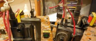
During one of my visits to the radio market, I managed to buy several printed circuit boards from decommissioned equipment practically for a song (Fig. 1). A power transformer was included with one of the boards. After searching on the Internet, it was possible to establish (presumably) that all the boards are from EPSON dot matrix printers. In addition to many useful details, the board has a good two-channel power supply. And if the board is not supposed to be used for other purposes, you can build an adjustable laboratory power supply based on it. How to do this is described below.
 The power supply contains channels +24 V and +5 V. The first is built according to the circuit of a step-down pulse-width stabilizer and is designed for a load current of about 1.5 A. When this value is exceeded, protection is triggered and the voltage at the output of the stabilizer drops sharply (short circuit current approximately 0.35 A). The approximate load characteristic of the channel is shown in Fig. 2 (black curve). The + 5V channel is also built according to the pulse stabilizer circuit, but, unlike the +24 V channel, according to the so-called relay circuit. This stabilizer is powered from the output of the +24 V channel (designed to operate from a voltage source of at least 15 V) and has no current protection, therefore, if the output is short-circuited (and this is not uncommon in the practice of a radio amateur) it may fail.
And although the stabilizer current is limited in the +24 V channel, in case of a short circuit, the switch transistor heats up to a critical temperature in about a second. The + 24V voltage regulator circuit is shown in Fig. 3 (letter designations and numbering of elements correspond to those printed on the printed circuit board). Consider the work of some of its nodes that have features or are related to alteration. A power switch is built on transistors Q1 and Q2. Resistor R1 serves to reduce power dissipation across transistor Q1. A parametric regulator of the supply voltage of the master oscillator is built on the transistor Q4, made on a microcircuit, designated on the board as 3A (hereinafter we will consider it as DA1).
Laboratory power supply diagram
 This microcircuit is a complete analogue of the TL494, famous for computer power supplies. Quite a lot has been written about its operation in various modes, so we will consider only some of the circuits. The stabilization of the output voltage is carried out as follows: to one of the inputs of the built-in comparator 1 (pin 2 of DA1) through the resistor R6, an exemplary voltage is supplied from the internal source of the microcircuit (pin 14). The output voltage of the stabilizer is supplied to the other input (pin 1) through the resistive divider R16R12, and the lower arm of the divider is connected to the reference voltage source of the current protection comparator (pin 15 DA1). As long as the voltage at pin 1 of DA1 is less than at pin 2, the switch on transistors Q1 and Q2 is open.
As soon as the voltage at pin 1 becomes greater than at pin 2, the key closes. Of course, the key control process is determined by the operation of the master oscillator of the microcircuit. Overcurrent protection works in the same way, except that the output voltage affects the load current. The current sensor is resistor R2. Let's consider overcurrent protection in more detail. The reference voltage is applied to the inverting input of comparator 2 (pin 15 DA1). Resistors R7 are involved in its formation. R11 as well as R16. R12. As long as the load current does not exceed the maximum value, the voltage at terminal 15 of DA1 is determined by the divider R11R12R16.
Resistor R7 has a fairly high resistance and has almost no effect on the reference voltage. When overloaded, the output voltage drops sharply. In this case, the exemplary voltage also decreases, which causes a further decrease in the current. The output voltage drops to almost zero, and since now the series-connected resistors R16, R12 are connected in parallel to R11 through the load resistance, the reference voltage, and therefore the output current, also decreases sharply. This is how the load characteristic of the +24 V stabilizer is formed.
The output voltage on the secondary (II) winding of the step-down power transformer T1 must be at least 29V at a current of up to 1.4 A. The + 5V voltage stabilizer is made on the О transistor and the 78L05 integral stabilizer, designated on the board as SR1. A description of a similar stabilizer and its operation can be found in. Resistors R31, R37 and capacitor C26 form a PIC circuit for the formation of steep pulse edges.
To use the power source in the laboratory unit, you need to cut out from the printed circuit board the area on which the parts of the stabilizers are located (in Fig. 1, separated by light lines).
In order to be able to regulate the output voltage of the +24 V stabilizer, it should be slightly modified. First, you need to disconnect the input of the +5 V stabilizer, for which you need to solder the resistor R18 and cut the printed conductor going to the emitter terminal of the transistor Q6. If the +5 V source is not needed, its details can be removed. Next, you should remove the resistor R16 and connect the variable resistor R16 * instead (like other new elements, it is shown in the diagram with thickened lines) with a nominal resistance of 68 kOhm.
Then you need to solder the resistor R12 and solder it on the back of the board between pin 1 of DA1 and the negative terminal of the capacitor C1. Now the output voltage of the unit can be changed from 5 to 25 V. It is possible to lower the lower regulation limit to about 2V by changing the threshold voltage at pin 2 of DA1. To do this, remove the resistor R6, and apply the voltage to pin 2 of DA1 (about 2 V) from the trimmer R6 ’with a resistance of 100 kOhm, as shown in the diagram on the left (opposite the old R6).
This resistor can be soldered from the parts side directly to the corresponding pins of the microcircuit. There is another option - instead of resistor R6, solder R6 ″ with a nominal value of 100 kOhm, and between pin 2 of the DA1 microcircuit and the common wire, solder another resistor - R6 ″ ″ with a nominal value of 36 kOhm. After these alterations, the stabilizer protection current should be changed. After soldering resistor R11, solder in its place the variable R11 * with a nominal resistance of 3 kOhm with the resistor R11 included in the engine circuit ″. The bead of the R1 V resistor can be brought out to the front panel to quickly adjust the protection current (from about 30 mA to a maximum value of 1.5 A).
 With this inclusion, the load characteristic of the stabilizer will also change: now, when the load current is exceeded, the stabilizer will switch to its limiting mode (blue line in Fig. 2). If the length of the wire connecting the resistor R11 'to the board exceeds 100 mm, it is advisable to solder a 0.01 μF capacitor parallel to it on the board. It is also advisable to provide Q1 with a small heatsink. A view of the modified board with adjusting resistors is shown in Fig. 4.
Such a power supply unit can be operated with a load that is not critical to voltage ripples, which at the maximum load current can exceed 100 mV. You can significantly reduce the level of ripple by adding a simple compensation stabilizer, the diagram of which is shown in Fig. 5. The stabilizer is based on the widespread TL431 microcircuit (its domestic counterpart - KR142EN19). A regulating element is built on transistors VT2 and VT3. Resistor R4 here performs the same function as R1 in a switching regulator (see Fig. 3).
On the VT1 transistor, a voltage drop feedback unit is assembled to solder from the side of the parts directly to the corresponding terminals of the microcircuit. There is another option - instead of resistor R6, solder R6 ″ with a nominal value of 100 kOhm, and between pin 2 of the DA1 microcircuit and the common wire, solder another resistor - R6 ″ ″ with a nominal value of 36 kOhm.
After these alterations, the stabilizer protection current should be changed. After soldering the resistor R11, solder in its place the variable R11 * with a nominal resistance of 3 kOhm with the resistor R11 included in the engine circuit ″. The bead of the R1 V resistor can be brought out to the front panel to quickly adjust the protection current (from about 30 mA to a maximum value of 1.5 A). With this inclusion, the load characteristic of the stabilizer will also change: now, when the load current is exceeded, the stabilizer will switch to its limiting mode (blue line in Fig. 2). If the length of the wire connecting the resistor R11 'to the board exceeds 100 mm, it is advisable to solder a 0.01 μF capacitor parallel to it on the board. It is also advisable to provide Q1 with a small heatsink. A view of the modified board with adjusting resistors is shown in Fig. 4.
 Such a power supply unit can be operated with a load that is not critical to voltage ripples, which at the maximum load current can exceed 100 mV. You can significantly reduce the level of ripple by adding a simple compensation stabilizer, the diagram of which is shown in Fig. 5. The stabilizer is based on the widespread TL431 microcircuit (its domestic counterpart - KR142EN19). A regulating element is built on transistors VT2 and VT3. Resistor R4 here performs the same function as R1 in a switching regulator (see Fig. 3). On the transistor VT1, a feedback node is assembled for the voltage drop across the resistor R2. The collector-emitter section of this transistor must be connected instead of the resistor R16 in the circuit in Fig. 3 (of course, the variable resistor R16 'is not needed in this case).
This node works as follows. As soon as the voltage across the resistor R2 exceeds about 0.6 V, the transistor VT1 opens, which causes the comparator of the DA1 microcircuit in the pulse stabilizer to switch and, consequently, the closing of the key on the Q1.02 transistors. The output voltage of the switching regulator decreases. Thus, the voltage across this resistor is maintained at about 0.65 V. At the same time, the voltage drop across the regulating element VT2VT3 is equal to the sum of the voltage drop across the resistor R2 and the voltage across the emitter junction of the transistor VT3. ie about 1.25 ... 1.5V depending on the load current.
 In this form, the power supply unit is capable of delivering a current of up to 1.5A to the load at a voltage of up to 24V, while the ripple level does not exceed several millivolts. It should be noted that when the current protection is triggered, the ripple level increases, since the DA1 microcircuit of the compensation stabilizer closes and the regulating element is completely open.
The printed circuit board for this stabilizer was not designed. Transistor VT3 must have a static current transfer coefficient L21E of at least 300, and VT2 - at least 100. The latter must be installed on a heat sink with a cooling surface area of at least 10 cm².
Establishing a power supply with such an addition consists in selecting the resistors of the output divider R5-R7. With self-excitation of the unit, you can bypass the emitter junction of the transistor VJ1 with a capacitor with a capacity of 0.047 μF. A few words about the +5 V channel stabilizer.
It can be used as an additional source if there is an additional 16 ... 22 V winding in the T1 transformer. In this case, another rectifier with a filter capacitor is needed. Since this stabilizer does not have protection, the load must be connected to it through an additional protection device, for example, described in, limiting the current of the latter to 0.5 A. current, for example, on an operational amplifier, as is done in.